This thread has been locked.

If you have a related question, please click the "Ask a related question" button in the top right corner. The newly created question will be automatically linked to this question.

TPS65631W discharge time

Other Parts Discussed in Thread: TPS65631W, TPS22860, SN74LVC1G132, SN74AHC1G00

Hi

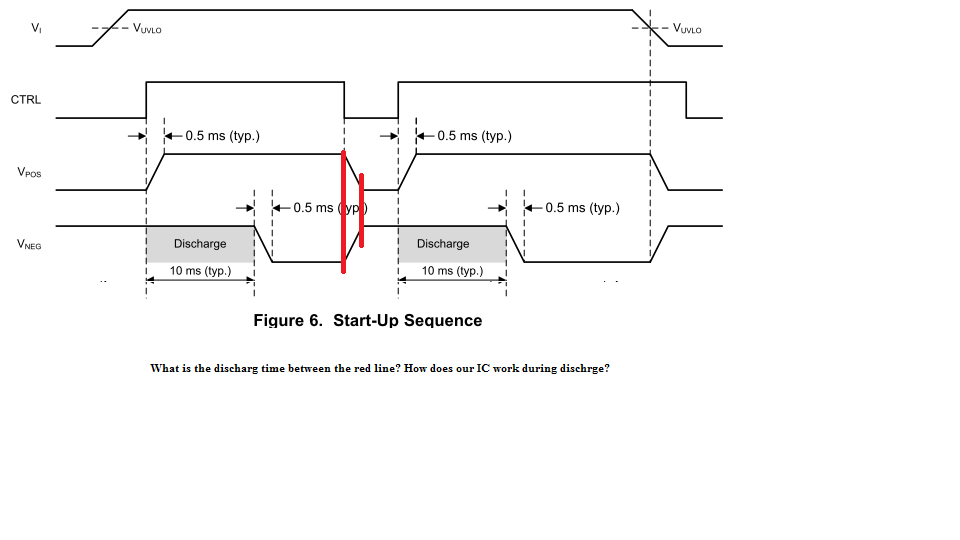
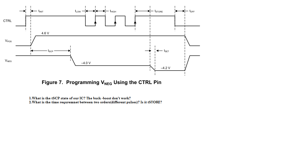
I have a customer making smart watch. They have chosen two AMOLED supplier, one is  RM69080, the other is RM67160. The two AMOLED Displays need differnt Power Supply. For RM69080, it need slow discharge, or it will flash, and they use RT4723A. For RM67160, they need fast discharge, or it will meet short internally. 

Can we promote TPS65631W to them to meet the two different discharge requirement? How can it adjust the discharge time? Thanks.

Best Regards

Janet

  • Hello Janet,

    What are the input and output voltages and the output current? Could you please precise as well the discharge time requirement?

    Best regards,

    Diaara

  • Hello Diaara,

    The input is from battery, which ranges from 3.4V ~4.25V; Vposis 4.6V, Vneg is -2.4V.  The TPS65631W is controlled by driver IC through CTRL pin.

    They didn't tell me the  discharge time requirement and they let me to provide the discharge working method and the time our IC needed to discharge.

    I also listed several other questions in below pictures. Could you help with this? Thanks. The customer is doing smart watch and their volume is around 500ku.

  • Hello Janet,

    Yingying Sun said:

    I also listed several other questions in below pictures. Could you help with this? Thanks. The customer is doing smart watch and their volume is around 500ku.

    When the CTRL pin goes low, the outputs are high impedance. This means that the control of the discharge is not implemented. However it is possible to implement that function with external components.

    Yingying Sun said:

    1) When an error condition is detected, the device goes into shutdown and the input and outputs are disconnected. The different error conditions are listed in section 8.3.6 (Short Circuit Protection) of the datasheet.

    2) At least the maximum value of tsore is needed before you send another pulse package.

    Yingying Sun said:


    With D2, current can flow only when Vneg is negative enough. Our IC do not need the diode. Where is this picture from?

    Best regards,

    Diaara

  • Diaara

    About the dischrge, you said it is possible to implement that function with external components. could you help provide the discharge circuit? like RC?How to determine the component values?

    Besides, below is the schematic, could you help check?

    LSD7PW-TPS65631_V01.01.pdf

  • Hello Janet,

    You can add a resistor in parallel to the output capacitor for example. Its value will then depend on the discharge time you want to have. It will take approximately 3RC for complete discharge. For instance, if your discharge requirement is 10 ms and the output capacitor is 10 uF, then you will need R= 333 Ω. The value of R will be limited by your load and the maximum output current (0.2 A), Iload + Idischarge ≤ 0.2A.

    Another method would be to add at the output a switch controlled with the CTRL signal. This switch would be on when CTRL goes low.

    I checked your schematic and it seems ok to me, but the diode D1 is not necessary for our IC. 

    Best regards,

    Diaara

  • Diaara
    About adding switch method, the ctrl is used to control the switch. Another problem is that except discharge, driver IC will also send pulses to adjust the negative voltage which will affect the switch state,too. How to solve that? Thank you.

    Best Regards
    Janet
  • Hello Janet,

    To solve this, I propose to use the circuit below. The values of the RC filter components were selected such that all frequencies higher than 1 kHz are filtered. Therefore the pulses whose durations are between 2 us and 25 us will be filtered.

    This will allow you to generate a new signal CTRL1 to control your switch.

    Best Regards,

    Diaara

  • Diaara

    Thanks for your support. I have atatched the schematic in below. Could you  help check whether it is OK? Thanks.

    4721.LSD7PW-TPS65631_V01.01.pdf

  • Hello Janet,

    I reviewed your schematic and I think you have 2 problems in it related with the TPS22860. First, I think that this device will not work as you want here because on its datasheet it is told that when th ON signal goes low Vin to Vout is off (page 7). Another thing is that with the way you use in the OUTN output you may damage the internal components of the TPS22860.

    I will come back to you later with suggestions on how to solve this.

    Best regards,

    Diaara

  • Diaara
    For the first problem, I think we can use a and logic instead of 1G04, for the negative voltage, can we use a Mosfet? It looks like the load switch can't endure negative voltage. If we choose the mosfet, which part do you recommend?

    Looking forward for your reply. This project is urgent for us to win. We need to accelerate the progress. Thanks.

    Best Regards
    Janet
  • Hello Janet,

    I propose to use the circuit below for the discharge:


    I also noticed that you are using the NAND gate SN74AHC1G00, I would recommend to use the SN74LVC1G132 instead in order to avoid having jitters on your signal CTRL1.

    Best regards,

    Diaara


  • Diaara
    Thank you so much for your continuous support. Just one more question, do we adjust the resistor R5 to adjust the discharge time ?

    Thanks you so much.
    Best Regards
    Janet
  • Hello Janet,

    Yes, you adjust the resistor R5 to meet the discharge time requirement on OUTN and R2 for OUTP. It will take approximately 3RC for complete discharge.

    Best regards,

    Diaara