This thread has been locked.

If you have a related question, please click the "Ask a related question" button in the top right corner. The newly created question will be automatically linked to this question.

LM3150 webench circuit not working as expected

Other Parts Discussed in Thread: LM3150

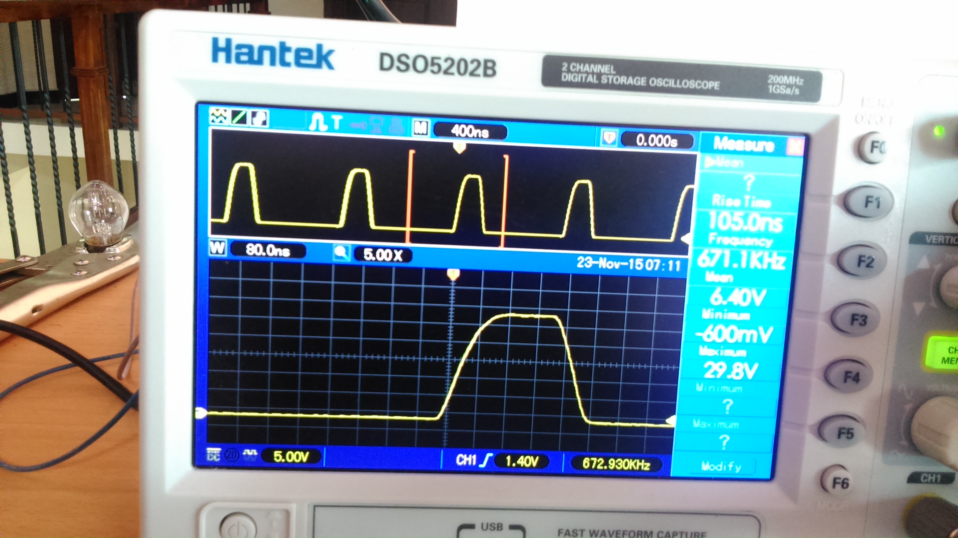
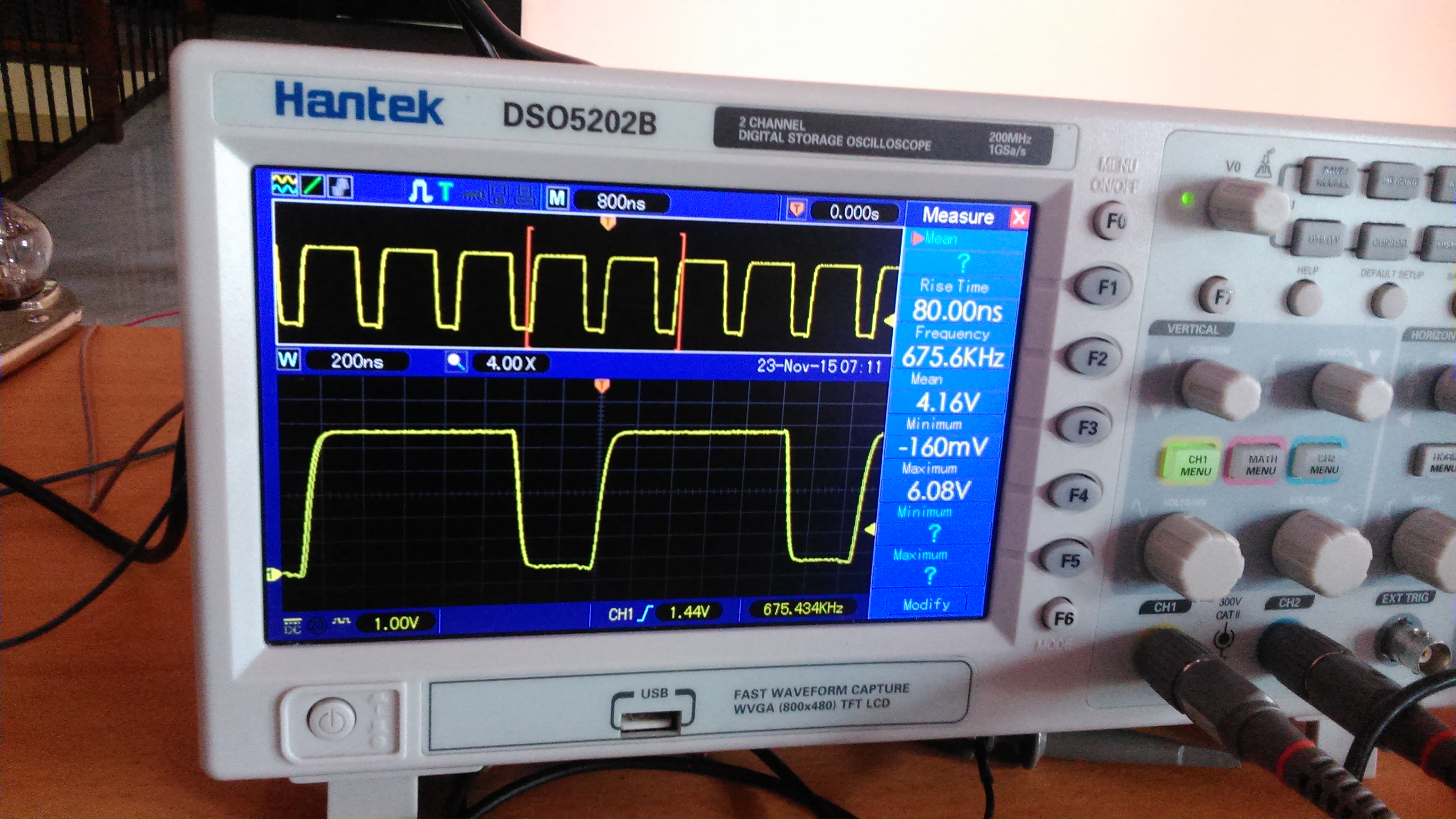
I designed the  below circuit Using webench designer. Designed a PCB and assembled the components. When I powered it up the LM3150 heats up very rapidly. The out put has ripples of about +/- 0.5V.  Also there is an audible  noise coming out from the circuit.  What could be the reason for this ?

final 5V 5A.pdf

  • Hi Michel,

    Thank you for your question! I will redirect your post to the appropriate thread for expert advice.

    Thanks,
    Anston
  • Hi Michel,
    Do you see this behavior at any level of output current or is it only at full load?
    Thank you,Florent Boico
  • I did not check for full load. I checked for
    1. No load
    2. LED
    3. Motor

    The LED and Motor drew small currents in the range of 100 mA.
    I observed a reduction in ripple when i placed my hand on the IC too
  • Hi Michel,
    I reproduced the webench circuit using the LM3150 standard EVM as a template except for the FETs which I left unchanged and the inductor which is a coilcraft XAL7070-472 with 4.7uH and 13mohm instead of the one given in webench (due to part availability). It looks like the circuit is functionning pretty well and is stable from 0A to 5A at 25Vin.
    Can you share your layout regarding the power circuit? These power systems are noisy by nature and so are very sensitive to layout so it could be that the feedback is picking up extra noise from the switching events.
    Thank you,Florent
  • power cct.brdpower cct.sch

    I have attached the eagle files to your perusal. I have mounted the same components as given in the webench design

  • Hi Michel,

    I see an issue with the ground connection. I'm trying to find the ground connection between the output capacitor and the input capacitor. I can see it's connected but I cannot find the dedicated path.

    Typically, the input and output capacitor's GND should be relatively close. Also, the GND connection from the bottom FET (Q8) to the output capacitor is very long and has a long length that is not shared with the path from the output capacitor to the input capacitor. When the converter switches, large currents rush through those traces and the stray inductance will create problems. Having all the return current from Q8 go under the controller (U8) is also not recommended.

    Typically, Cin and Cout would be closer together, and the source of Q8 should be closer to Cout's GND. You could try lifting the source pins of Q8 and connect them with a short wire to Cout and do the same between Cout and Cin to offer a different path and see if that helps.

    By the way, are your FETs damaged?

    Best Regards,
    Florent
  • Hi Florent,

    Thanks for the Advice.
    I connected the wires as you told and I could get the 5V output. under no load conditions. The MOSFET output was a near perfect rectangular waveform.

    But the controller(U8) heats up upto 55 Centigrade. Is this normal? 

    Furthermore, when I connect a load (LED) to the output, the temperature increases rapidly beyond 75 Centigrade.

  • Hi Michel,

    I'll need to look in the details of the normal power dissipation for this part. That being said, 75C at room ambient temperature seems hot. Especially given the fact that the IC is a controller. That means that the power it dissipates is only that necessary to charge and discharge the gates of the FET during the switching events. It could still be consequential depending on the switching frequency and the gate charge of the FETs used but at a glance I'd say it feels high.  Do you have a way of measuring what the actual switching frequency is?

    Thank you,

    Florent

  •   

    HG pin output

    LG pin output

    The switching frequency is around 675Khz