This thread has been locked.

If you have a related question, please click the "Ask a related question" button in the top right corner. The newly created question will be automatically linked to this question.

TPS43061

Other Parts Discussed in Thread: TPS43061

Hello,

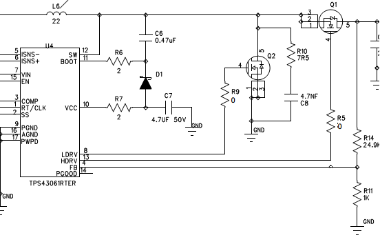
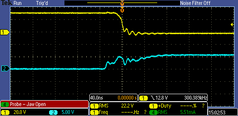
My customer is using P/N: TPS43061 boost converter as shown below. It seems like the IC or transistors continually failing.  The LDRV and HDRV signals are sometimes both high simultaneously as shown in the attached screen capture (Channel 1 is HDRV and channel 2 is LDRV).  Please advise.

Thanks,

Mehrdad.

  • Hi Mehrdad,

    First I want to confirm that CH1 is in fact HDRV and not SW. If it is actually SW this is normal operation. When HDRV goes low the body diode of the high-side MSOFET conducts so SW is still at ~VOUT. When LDRV goes high the low-side MOSFET turns on and pulls down SW. If this is HDRV I have never seen anything like this before. There should be a dead-time between HDRV starting to go low and LDRV starting to go high.

    Can you also share:

    1. Input voltage, output voltage, load current
    2. Part numbers for the MOSFETs
    3. PCB layout

    Best Regards,
    Anthony

  • I called the customer.  

    The TPS43061 has “adaptive deadtime”.

    Although not shown in the block, the IC looks at each gate output and the SW node.

    It adjusts the gates based on where SW is.

    Adaptive also means the typical 65ns can be varied, notice there is no MIN MAX, only a typical for the overlap delay.


    Must have the mosfets gates connected for the waveforms to be correct.

                You mentioned your pictures were with the top fet replaced by a diode.

                This will not give the proper signals into the IC for adaptive delay.


    This picture from the EVM users guide shows it well.

    This is from the EVM, its what you should see, if you don’t then something is wrong with your test equipment.

    The circled area shows where top fet body diode is conducting.

    At 400ns per division this is about 65ns on each delay.


    1.    Low fet turns off

    2.    Inductor current must continue so SW rises and current flows through the top fet body diode.

    3.    Sees SW high and has satisfied the 65ns typical delay so it then turns on the top fet.

    4.    Top fet turns off and current flows in its body diode.
    You can see SW slightly higher during body diode conduction.

    5.    Bottom fet turns on after 65ns and “force commutates” the top fet body diode off.