This thread has been locked.

If you have a related question, please click the "Ask a related question" button in the top right corner. The newly created question will be automatically linked to this question.

BQ25010 getting extremely hot, stays hot not charge the battery

Other Parts Discussed in Thread: CC2541, BQ25010

Hi, 

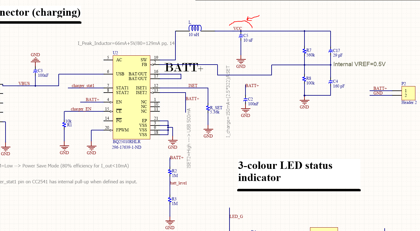
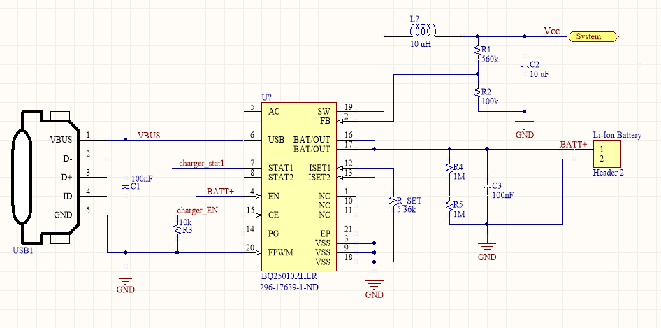
I am using BQ25010RHLR to charge the battery and provide 3,3V supply voltage for my Bluetooth unit. 

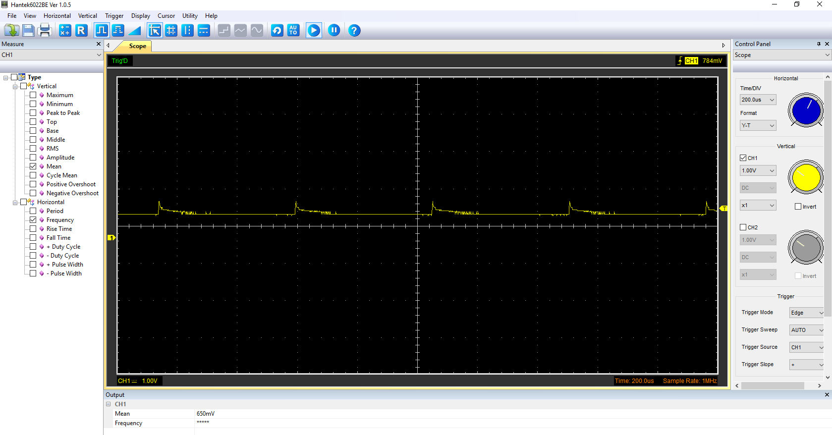
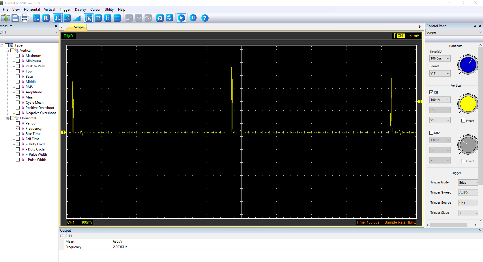
when  I connect the USB to charge the battery it does not  charge the battery, it does not provide the 3.3V and the feedback reference voltage is 0V. 

I checked that the 5V of the USB bus reaches the IC. 

Now when I connect the VCC to 3V (look at the attached screenshot) it gets hot (80 C). and again the battery would not charge. 

I did enable the charger by pulling down CE pin (by micro-controller cc2541). 

This happend in all of my samples.  

  • Hello Kamyar 

    Can you please measure the following?

    - Circuit is not powered, FB pin to GND with and without the IC populated on the board

    - Circuit is not powered, VCC to GND

    - With USB connected, please capture SW pin to GND with scope

    - With USB connected, please capture BATT+ to GND

    - With USB connected, please measure ISET1 to GND

  • Hi Kalyan, 

    Thanks for the reply, 

    Following are the outcomes:

    -Circuit is not powered FB to GND without chip 101kohm, with chip 83.6kohm. 

    -Circuit is not powered , VCC to GND with chip 15 ohm (0.015kohm) !!, without chip 590kohm. 

    -SW with USB connected is exactly zero with 10 mV spikes (very small)

    -BATT+ to GND (No Batt connected) figure below:

    -ISET1 to GND is figure below:

    Please let me know if i miss understood any of your test actions. I would redo them if needed. 

    The VCC to GND is suspiciously  low when the IC is presented. 

    All the Best, 

  • Kaymar

    You are correct. The value looks really low. We are repeating the measurements on our side and should have some suggestions for you today.
    In order to make sure there is no set up issue on your side, if you have a bq25010 EVM, please check resistance measurement on the equivalent of VCC point.
  • Kaymar,

    I used a bq25010 EVM and took these measurements without power applied.

    FB to GND 95k (schematic shows 100k)

    VCC to GND (top or FB resistor divider) 116k (schematic shows 261k + 100k)

    System charges on AC1 at 500mA.

    I will continue to investigate to compare your results with an EVM.

    Regards,

    Dick

  • Thanks Dick, 

    I have to add that All the information I have provided was with charger without battery connected. The reason is the battery's terminal would be short circuited (As I said the BAT to ground is shorted when the chip is placed). I have 15 chips and they all suffer from same problem. 

    Thanks for your time and investigation, I will be waiting for your response. 

    All the Best, 

  • Kamyar,

    One basic question that I have to ask.  C3 on the schematic you sent is polarized and is connected backwards.  I expect that is not the case.

    I've done a bit more testing on the bq25010 EVM.  This is with the battery set to 4.2V and the EN pulled low.  The switching frequency is as expected.  (Channel 1 is BAT and Channel 2 is SW.  Since you are not even able to test with the battery, I'm not sure how much this will actually help.

    Do you have one of the bq25010 EVMs?  I would suggest testing one of the EVMs to verify its functionality.  Then, take the failing IC from your board and placing it on the EVM - this will prove / disprove if it is a part problem.  Based on you note that all parts have failed, I doubt it really is an IC issue.

    I have reviewed the schematic again and nothing seems incorrect.

    Dick

  • Hi Dick, 

    C3 is a ceramic cap and the mistake is only in the schematic graphic level. I really appreciate the tests and the time that you went through. 

    As I said I don't have the EVM board and I am not sure how that is going to help me. 

    Based on information that I provided and measurements of the board without IC I am rolling out any short circuits and mistake in production process (of PCB board). 

    I am currently bewildered what can be wrong!!!!

    But once again thanks for your time and feedback.

    All the Best,


  • I know this thread is a little old. However, I am attempting to solve this problem on behalf of Kamyar and am hoping you can answer some questions I have come up with.

    First, I have simplified the schematic to show the changes we have made:

    The issue we are having at the moment is that the PWM signal seen at the SW output has a 12% duty cycle, giving us only 0.7V at Vcc for our system and approx. 0.1V at the FB pin (which should be 0.5V). This happens with the battery connected and with or without the USB plugged in. We have verified that the USB does charge the battery just fine.

    My questions are:

    1. In your last post you mentioned that you pulled EN low to get the wave forms you show, but when I pull EN low I get nothing out of the SW output. This also means that I have removed the battery, so ISET2 is left floating. Also, from the documentation, pulling EN low puts the DC-DC converter into shutdown mode. Should EN be high or low for battery operation? And is using the battery voltage wise or unwise for setting EN in your opinion?

    2. R4 and R5 are used to measure the battery level (sent back to the microcontroller from the midpoint), would having them connected as they are have any adverse effect?

    3. The Vcc is used in multiple locations on the rest of the board, and current draw can be over 150mA (depending on the code running on the microcontroller). If the system is trying to draw more current than the chip allows, would that result in the reduced duty cycle of the SW pin?

    Thank you in advance for any help or guidance you can provide.

    -Phillip

    PWM at SW: