This thread has been locked.

If you have a related question, please click the "Ask a related question" button in the top right corner. The newly created question will be automatically linked to this question.

LM3429 PWM dimming problem

Other Parts Discussed in Thread: LM3429

Dear ,

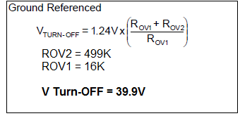
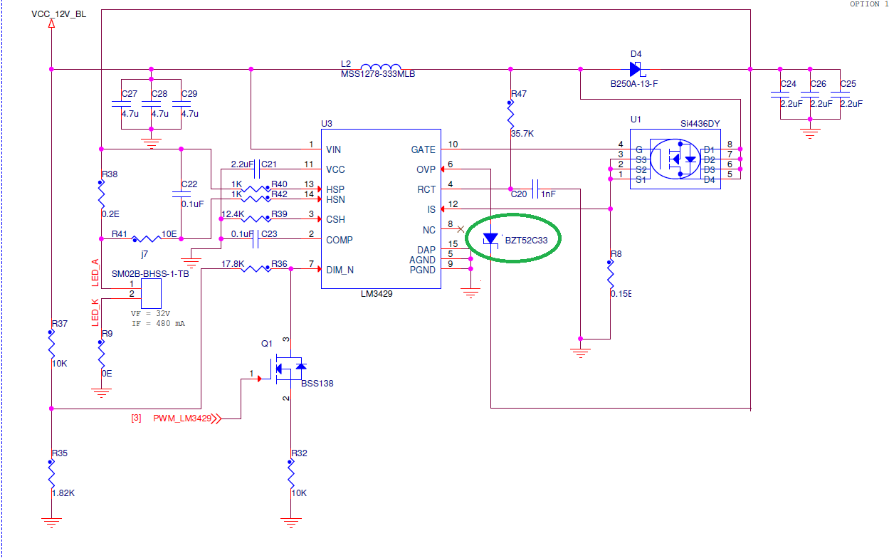
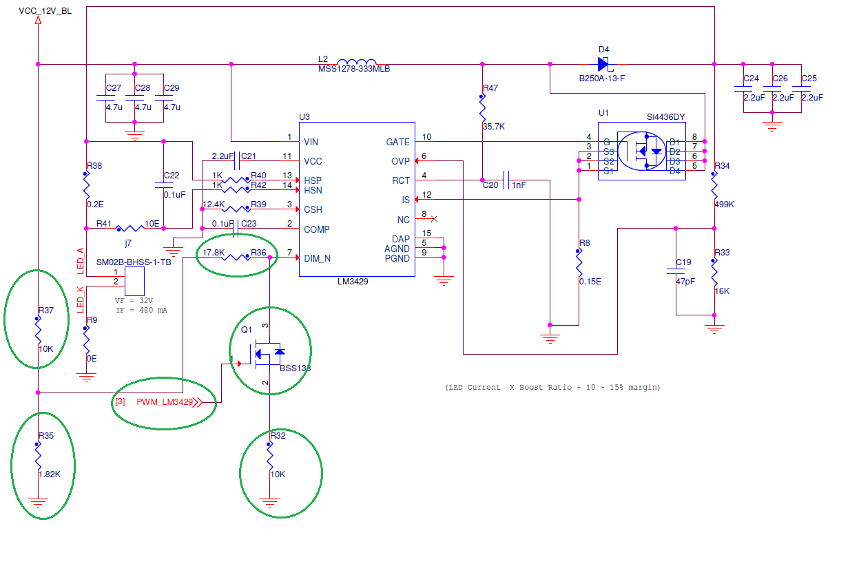
Here I'm facing one problem. The LCD is not displaying data by default. When I probe pin DIM_N (pin number 7) using multimeter then only LCD is displaying data properly. Could you please review my schematic and let me know that whether my PWM connection is proper or not ?

Regards,

Azlum

  • Have you tried shorting R32? Q1 should pull nDIM to ground. Perhaps the extra load of the multimeter is allowing it to pull low enough, but the 10k resistor is preventing that otherwise?
  • Dear Clinton Jensen,

    R32 shorted and tried. But still result is same.

    I hope the working of nDIM pin is like below.

    Case_1 : When Q1 gate is low, drain and source continuity will be disconnected and resistor divider (due to R37 and R35) voltage is feeding to the nDIM pin. Thus the LEDs are blinking.


    Case_2 : When Q1 base is High, zero voltage from ground is feeding into the nDIM hence it is not blinking.

    Consider case_1, what is the minimum voltage is need to nDIM pin to make LED blinking ? It should be more than 1.2V or less ?

    Regards,
    Azlum
  • Have you proved the nDIM pin with a 10x voltage probe to check the levels? When Q1 gate is high the nDIM pin voltage should be near ground (at least below 100mV or so) and when the gate is low the nDIM pin should be above 1.28V. It's also good to probe to see if there is noise that could affect it. If you are borderline and there is a lot of noise it could behave incorrectly.
  • Dear Clinton,

    I have removed the Q1 and I'm getting 2.2V at nDIM pin. i,e more than 1.28V. This case the LCD should shows something on the LCD. But I'm couldn't see anything on the LCD.

    Also, what is 10x voltage probe ? I didnt understand. Could you explain little more ?

    Regards,
    Azlum
  • Dear Clinton,

    The back light is up. But still here I facing some problem, anything couldn't displayed on the LCD even though the back light is UP. When I drive nDIM pin from “Low” to “High” then only LCD could display data for fraction of time . i,e LCD displays data only while LOW to High transition time and again it go off. Could you suggest what might be the reason ?

    Here I have attached the video of this issue.


     Zip file of this video :- 

    LM3429_TEST VIDEO.zip

    Regards,

    Azlum

  • I really don't know the overall system well enough. If the LEDs are lit but the display isn't working it could be any number of things. It's possible the switching of the converter is interfering with something else completely.
  • Dear Clinton Jensen,

    I feel PWM side is causing problem. The display is working in back ground. When we drive the PWM pin from "Low" to "High" then only we can the LCD display in transition time .

    When we remove N-channel transistor, then I'm getting 1.8V in nDIM pin. In this case also the LCD should work properly. Is it ?

    Regards,
    Azlum
  • With 1.8V on nDIM it should be on. Do you have enough input capacitance to prevent the input supply from dipping when you turn the LM3429 on? Also, did you add extra hysteresis (using Ruvh) as recommended in the input undervoltage lockout section of the datasheet? That can help prevent errant uvlo conditions due to transients.

  • Dear Clinton,

    I have used RUVH is 17.8K. Hope this is more sufficient. How much is the required current in nDIM pin ? RUVH may prevent sufficient flow of current and causing the problem ? I'm really wondered with this issue. Even I have used less than 17.8K values and tested. It didn't help me.

    Regards,
    Azlum
  • Those values should be fine. So first off, do you have an oscilloscope to look at the nDIM pin with to make sure the signal is correct? By a 10x probe I just meant a high impedance type like 1Mohm or 10Mohm voltage probe, not a 50ohm one which would load things. So some other questions:

    1. Could you also probe the output voltage to make sure it isn't going into OVP? I'm not sure your exact setup but things like very long leads from the converter and throughout the LED string can cause overshoots on the output voltage.

    2. Do you have pictures of the layout and could you let me know what kind of lead lengths you have between the converter and the LEDs?

    3. Is the output capacitor located close to the regulator circuit?

    The first one (and third actually) could be verified by removing the upper OVP resistor so it cannot go into OVP. But a poor layout could cause all kinds of other issues including false triggering of UVLO, OVP, current limit, etc... If there are long lead lenghts between the LEDs and the regulator that is ok, it just needs to be accounted for in the design.

  • Dear Clinton,

    Please find the in-line reply. 

    Those values should be fine. So first off, do you have an oscilloscope to look at the nDIM pin with to make sure the signal is correct? By a 10x probe I just meant a high impedance type like 1Mohm or 10Mohm voltage probe, not a 50ohm one which would load things. So some other questions:

    <<Azlum>> Please find the attached image “nDIM.JPEG”. I’m getting more than 1.24V at nDIM pin. Also it is very stable voltage.

    nDIM.zip

    1. Could you also probe the output voltage to make sure it isn't going into OVP? I'm not sure your exact setup but things like very long leads from the converter and throughout the LED string can cause overshoots on the output voltage.

    <<Azlum>> Please find the images “ output_1, output_2, output_3”. These are the wave forms of the output. Since it is sawtooth wave, I have marked the output 3 different levels. OVP calculation is below for my circuit. 


    Output.zip

    2. Do you have pictures of the layout and could you let me know what kind of lead lengths you have between the converter and the LEDs?

    <<Azlum>> Please find the layout files. It is .brd format. You can see the layout in Allegro viewer.  

    iW-PREWV-BF-01-R1.0-REL1.0.brd

    3. Is the output capacitor located close to the regulator circuit?

    <<Azlum>> Yes, C24, C25, C26 are the bulk output capacitor which is closed to Anode and cathode terminals.

    Schematic:-

    iw-prewv-cs-01-r1_0-rel0_2.pdf

    The first one (and third actually) could be verified by removing the upper OVP resistor so it cannot go into OVP. But a poor layout could cause all kinds of other issues including false triggering of UVLO, OVP, current limit, etc... If there are long lead lenghts between the LEDs and the regulator that is ok, it just needs to be accounted for in the design.

  • Dear Clinton ,

    Please find my in-line reply. 

    Those values should be fine. So first off, do you have an oscilloscope to look at the nDIM pin with to make sure the signal is correct? By a 10x probe I just meant a high impedance type like 1Mohm or 10Mohm voltage probe, not a 50ohm one which would load things. So some other questions:

    <<Azlum>> Please find the attached image “nDIM.JPEG”. I’m getting more than 1.24V at nDIM pin. Also it is very stable voltage.

    7206.nDIM.zip

    1. Could you also probe the output voltage to make sure it isn't going into OVP? I'm not sure your exact setup but things like very long leads from the converter and throughout the LED string can cause overshoots on the output voltage.

    <<Azlum>> Please find the images “ output_1, output_2, output_3”. These are the wave forms of the output. SInce it is sawtooth wave, I have marked the output 3 different levels.

    2063.Output.zip

    OVP calculation given below :-

    2. Do you have pictures of the layout and could you let me know what kind of lead lengths you have between the converter and the LEDs?

    <<Azlum>> Please find the layout files. It is .brd format. You can see the layout in Allegro viewer.  

    Board File:-

    7853.iW-PREWV-BF-01-R1.0-REL1.0.brd

    3. Is the output capacitor located close to the regulator circuit?

    <<Azlum>> Yes, C24, C25, C26 are the bulk output capacitor which is closed to Anode and cathode terminals.

    Schematic:-

    7776.iw-prewv-cs-01-r1_0-rel0_2.pdf

    The first one (and third actually) could be verified by removing the upper OVP resistor so it cannot go into OVP. But a poor layout could cause all kinds of other issues including false triggering of UVLO, OVP, current limit, etc... If there are long lead lenghts between the LEDs and the regulator that is ok, it just needs to be accounted for in the design.

  • The output pictures make it clear, you are going into OVP. I know you set the level at 40V, as you can see it goes up to 45V (not uncommon given internal delays and the small delay caused by the 47pF cap) then turns off. The hysteresis is set at 10V so it should turn back on at 30V input which it does. That triangle wave is not due to the device switching as it is way to big and only at about 8Hz. So your LED string voltage must be higher than you think it is. You could test the easily by removing the 499k OVP resistor and see if it works, then you can measure your actual output voltage if it does. Sometimes LED forward voltages are specified at a certain die temperature, but they are always higher when cold and drop as they warm). I also noticed that you have your current limit set at only 1.6A, that is pretty close for this application. I would give more headroom and lower R8 to 0.1ohm or less so you don't run into current limit issues (if you do the output current will drop, particularly if you lower Vin).
  • Dear Clinton,

    I have removed 499K and tested. Still I cannot see anything on LCD. The required minimum back light LED voltage is 32V as per LCD data sheet. But when connected the LED’s anode and cathode (i,e load) to the driver IC output the expected voltage showing in the multitier is 28V (i,e expected voltage is not coming in the multimeter).

    1) How can I maintain the 32V with 499K removed condition ?

    2) Can I remove R33 and R34, then connect 32V zener diode across U3.6 and D4 cathode side (as below )? Is this good to try ?

    Regards,

    Azlum

  • Ok, you shouldn't need to remove the 499k and a zener will not work correctly since the OVP pin will try to source current when the threshold is exceeded. The RC should be fine and 499k is probably fine.

    However, I was able to get Allegro to look at your layout file. Unfortunately it has a lot of issue, enough that I don't believe it would ever work correctly even if the circuit design was perfect. Layout is very critical for switchers as they generate a lot of noise so routing and grounding have to be carefully done. I'll list out some of the major issues I noticed (some or all of which could cause major problems):

    1. The RCT trace is run beneath the inductor. It's a good idea not to ever run lower voltage signal type traces beneath an inductor. It is shielded so it might be ok IF the resistor were close to the part, but as it is the resistor comes first before the trace that routes beneath the inductor so noise coupling into the RCT pin could happen.

    2. The LED and current sense traces are very small. Way too small to be carrying 480mA. You will be causing significant drops that could introduce errors and noise and could even fuse the traces after some time operating at full current.

    3. The switch current traces are very small in places. Of particular concern is the trace from the source of U1 to R8. This will be switching with peak currents over 1A. I'm surprised that trace hasn't already fused. Just as important is the routing of that trace. It, along with R8, are routed directly beneath all of the sensitive current sense traces of the IC. You essentially have a small radiating antenna blasting noise into those pins. It would be impossible to regulate current  with those interacting, and they will as routed.

    4. Vias. They are important. For low current signal traces like the OVP and RCT one via is fine if you need to go layer to layer. For high current traces like the LED and switching current traces you will absolutely need more, I usually suggest at least one per 250mA of current. For example there is only one via connecting L2 to U1. That will be switching at over an amp and that via will introduce a big drop, create excess noise, and will likely fuse eventually. I would not use less than 6 vias there. Grounding vias are important as well if you need to tie two critical ground points together from top to bottom (more in #5 on this) you should use as many as you can. Again, grounding is critical.

    5. There are serious grounding issues. The most important with a boost regulator is that the chip DAP/PGND, R8 ground, output capacitor grounds, and the LED string ground all be tied together as closely as possible using solid planes where you can. If some are on top and some on the bottom you still want to get them as close together as possible and tie the top and bottom ground planes directly together with multiple vias right next to the components. With them separated as much as they are in your layout you will have different ground potentials that can cause all kind of issues, sometimes even destructive. You are creating a discontinuous current switching loop so if the grounds aren't solid things bounce all over the place and you force high frequency current return paths all around the board that can create serious noise issues for any circuits near where that path is forced.

    In any case, I think your circuit is just fine and will work nicely when the layout is fixed. You can't easily test most of that out except the grounding. You could take thick, short wires and tie all those together to see if there is improvement, but the other issues may still prevent correct operation. There are app notes on the TI website (and others) that give layout guidlines for switching power supplies if you need more information than this. But fixing these should make sure any erroneous operation isn't due to the layout in the future.

  • One last note, the best thing you can do (if possible in your situation) is to use an internal solid ground plane. This would provide some shielding layer to layer and you could tie all your grounds to it closely together. It also provided a solid return path for the switching current (the return path likes to follow the path of least impedance, so it tries to follow the forward path very closely).