This thread has been locked.

If you have a related question, please click the "Ask a related question" button in the top right corner. The newly created question will be automatically linked to this question.

radiated emissions on TPS54360

Other Parts Discussed in Thread: TPS54360

Hi,

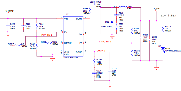
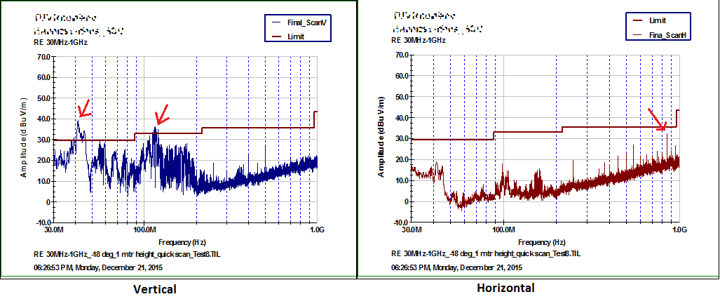
I am using TPS54360 in one of my projects and I have its radiated emission graph here. Could you please help me reduce it. We do not have luxury of space for inserting a common mode choke on the board.

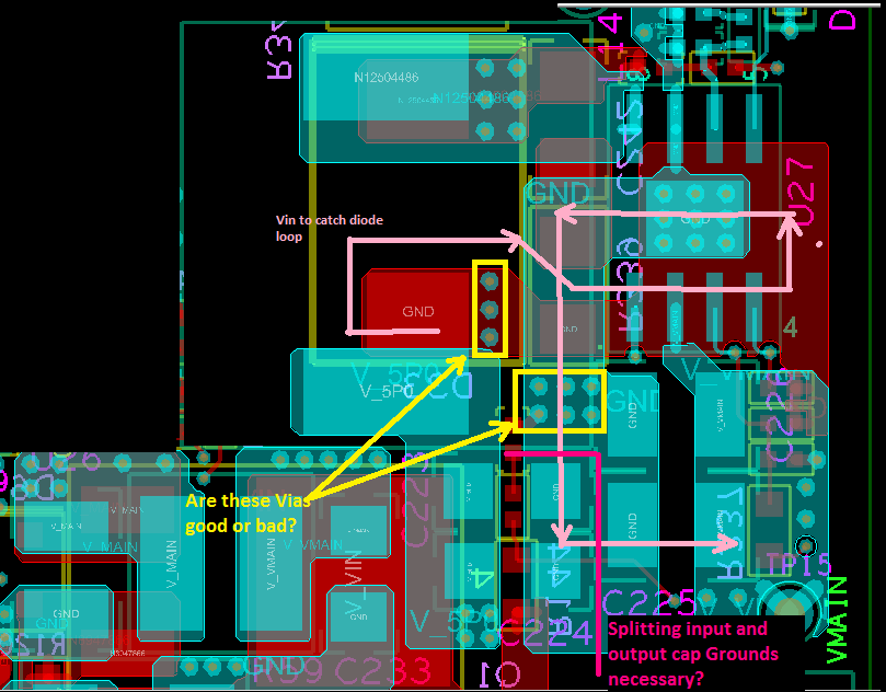
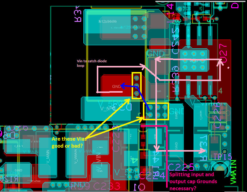
W have no traces running over plane splits to contribute to radiation and all the signals have at least one continuous ground plane adjacent to it.. 

The load is approximately 3A @5V.

Is snubber really recommended for TPS54360? else, will the snubber shown here contribute to radiation?
attached is the placement also

Green shows top layer and Red indicates bottom layer.

Thanks in advance

Abin

  • The first thing, is you need to correlate your radiated emission frequency to the signals in your circuit. What frequencies are causing you to fail? where do you see that frequency content occur? Typically, you may see as common frequencies, the switching frequency and its harmonics or possibly ringing frequencies on the SW node. if it is ringing on SW, then you can use an RC snubber to filter it. Also, can you post your schematic to cross reference against your layout?
  • Hi John,

    Here is the Schematics as well as the radiated emission readings.

    Regards,

    Abin

  • Hi Abin,

    I have also taken a look over this and the two things I see are:

    1. In the layout it would be better to keep the TPS54360, input capacitors and schottky diode all on the same side of the board to make the best low impedance connections between them. These three components are part of the critical switching loop that can create high frequency noise if there is extra inductance in it. If you need to use a two sided layout it is better to via the connection of the SW pin to the inductor.
    2. The snubber could be made stronger by increasing the capacitor and decreasing the resistor. This may help with the noise measured in the 100 MHz - 200 MHz range.

    Hope this helps.

    Best Regards,
    Anthony

  • Hi Anthony,

    Thanks for the suggestion.

    I have a few queries.

    1. Are the vias shown in yellow doing good or harm? The idea was to reduce the loop size of Vin to catch diode ground pin, recommended by datasheet. Otherwise it will be taking the path shown in dull pink. I know that keeping the Catch diode on top is ideal, but mechanical constrains doesn't let me do that. So my question is, does the via shown here create unnecessary current loops? PS:This is the best way I can place the components.


    2. A fellow engineer was recommending to split the ground  used for input bypass capacitor and the output caps. Does it help me in reducing the radiations? He was asking me to connect the new output cap GND island to internal Ground plane using vias. 

    I would like to have an improvement in radiated emission margin. Its on the margin now. Any response will be appreciated.

    Thanks in advance.

  • If you must keep the diode and TPS54360 on opposite sides, you should keep the vias by the diode. It is important to minimize the impedance between the ground of the schottky diode and the gnd of the input capacitors. The Vin to catch diode loop you have drawn is very long. Are these vias near the diode connected to the ground copper of the input capacitors? The blue ground shape doesn't look like it connects to the vias.

    Instead of moving the diode to the other side, how about moving the TPS54360 to the other side? This way you can minimize the size of the critical switching loop and not have to use vias which can add impedance.

    Lastly I do not see any benefit in splitting the grounds when it comes to radiated emissions. We typically keep a solid ground like you currently have.

  • Hi Antony,

    We have internal ground layers, to which the blue vias are connected from the diode ground pad. To enhance visibility, I had disabled the internal layers. The blue line indicate the possible shorter path than the dull pink lines which would have been the current path if the vias in yellow boxes were not there.

    Thank you.

  • Hello,

    Here is an improved layout for the TPS54360 we are using. The initial revision had high emissions on low frequencies (<50Mhz). The previous layout had been shared in the above comments. The emissions were been broad band starting somewhere below 30 MHz and spanning till 50 MHz. Used near field probes to make sure that it is the regulator circuitry, the source for emissions.

    Please provide suggestions that can improve this layout so that any chance of emissions can be minimized.

    Thanks in advance.