This thread has been locked.

If you have a related question, please click the "Ask a related question" button in the top right corner. The newly created question will be automatically linked to this question.

UCCx8C4x / Typical Off-Line Application

Guru 29720 points
Other Parts Discussed in Thread: UC2845AQ, UCC38C44, TL431

Hi Team,

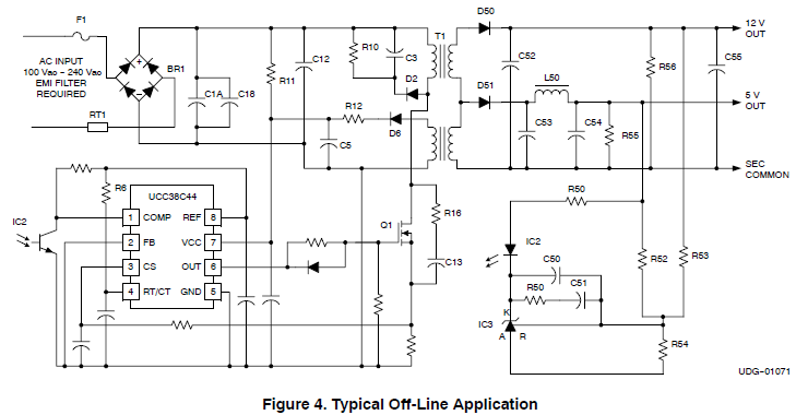
I found following "Typical Off-Line Application" for UCCx8C4x in datasheet page.9.
I would like to ask two questions about it.


question 1)
It seems there is no phase compensation capacitor and resistor around error amp for this application.
Is it no ploblem?

question 2)
My customer also considers to use UC2845AQ for automotive application.
Is it possible to use UC2845AQ for the same schematic(Figure 4) instead of UCC38C44?

Best Regards,
Yaita / Japan disty

  • In answer to your first question, the phase compensation for the application is formed around IC3 the TL431.
    C50,R50,C51 etc
    And in answer to your second question, the same schematic can be used in an automotive application with the UC2845AQ.
    Note that you will also need to replace the TL431 with its automotive equivalent,
    which is believe is
    www.ti.com/.../description
  • Hi John-san,

    Thank you for your helpful support!

    The following application shows FB pin is connected to GND, could you explain how to control the regulation in terms of  the red part in block diagram?


    Your help would be appreciated.

    Best Regards,
    Yaita

  • Is there any app note to explain the function of "Typical Off-Line Application(Figure 4)" ?
    Your support would be appreciated.

    Best Regards,
    Yaita

  • Hi Yaita,

    Because of the requirement for galvanic isolation between the primary and the secondary, it is not possible to feed the output voltage directly back to the FB pin. 

    What is typically done is that the error amplifier is placed on the secondary side, and the output of this amp is fed back to the primary side via opto coupler where it directly controls the COMP pin. (A further simplification is made by using a TL431 or similar as the secondary side error amp, which integrates the referance and amplifier function into one three pin package.)

    The internal error amp of the IC is not used in this case and the FB pin is grounded. Grounding the FB pin sends the output of the amp high, and it is pulled down by the opto coupler feedback as necessary to control the output voltage.

    This is mentioned in the pin assignments section of the datasheet.

  • Hi Billy-san,

    Thank you for your answer!

    Best Regards,
    Yaita