This thread has been locked.

If you have a related question, please click the "Ask a related question" button in the top right corner. The newly created question will be automatically linked to this question.

LM3489 Heating

Other Parts Discussed in Thread: LM3489

Hello,

I'm working on a buck converter 24V to 12V @ 3A and I decided to test this part.

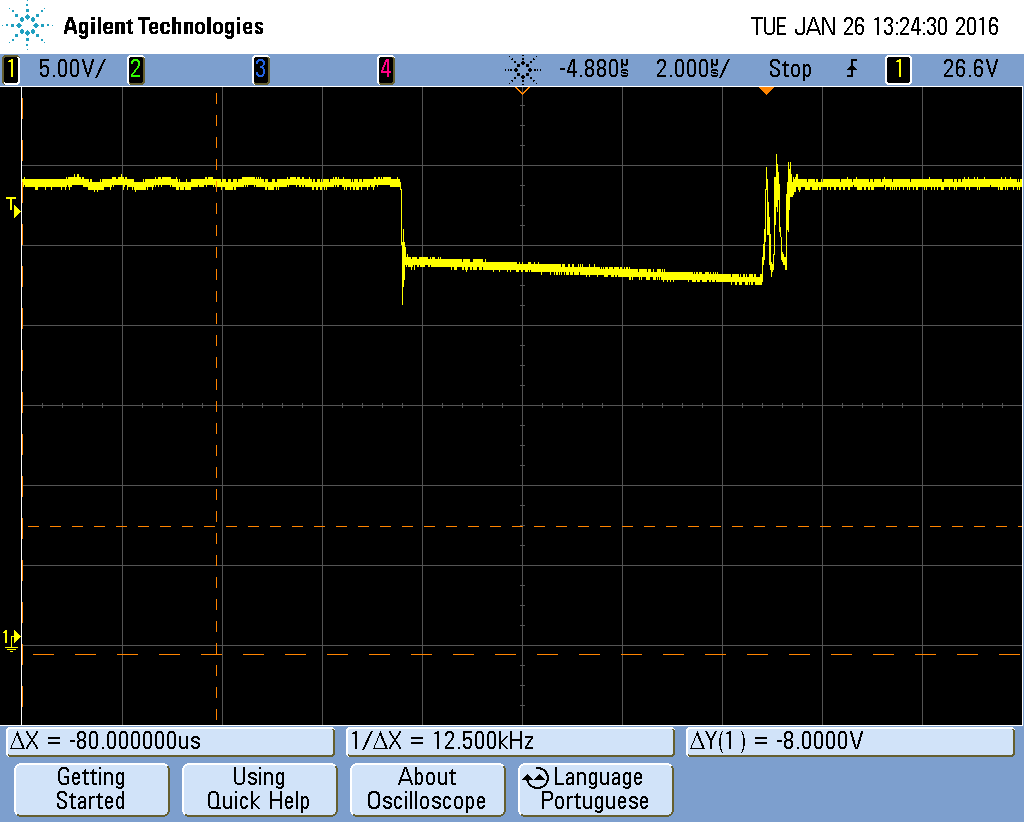
Without load, when I turn on the circuit, the output becomes in the target voltage and everything is good.

When I put any load, like for 100mA, the LM3489 heats a lot, jumps to 150 °C. The output voltage remains in the same level (12V). The only thing that I find that could heat the part would be the high frequency of switching.

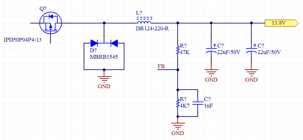
I measured 1Mhz while it should be about 300 kHz using the formula (1/(2*pi*R1*CFF) = FSW/10

Why is this frequency in this high value? I tryed put it down changing the Cff but without success. I'm using 100pF now.

  • Hello,

    I could not make it work following the datasheet or WEBENCH, because the system heating a lot in that way. Instead of put the Cff capacitor in the up resistor from feedback network, I added a 2.2nF in the down resistor, it brings the frequency to 100kHz and I have currents up to 2.5A.

    But, above that, I have considerable heating in the mosfet.

    In the image below, I have the PGATE signal and the ripple in the rise signal is the cause of extra heating.

    Does someone have any idea to eliminate this? Or is it intrinsic of hysteretics buck controllers?

  • Hello Anderson,

    Regret the late reply to your first post.

    The operating frequency (F) in the hysteretic buck controller is determined by knowing the input voltage, output voltage, inductor, VHYST, ESR
    (Equivalent Series Resistance) of output capacitor, and the delay. You can find the equation in the page 10 of the datasheet.

    Can you share your schematic if possible?

    We use the CFF cap to inject the vout ripple straight into the FB node bypassing the high side feedback resistor. This will lead to an increase in the switching frequency.  By taking the Cff out, you Fsw will drop significantly.

    What is the PFET you are using in the schematic?

    Regards,

    Sourav

  • Hello Sourav,

    Thanks for your answer. I'm doing the prototype, but the output stage is shown below.

    As I said, I needed to put a capacitor below to decrease the frequency. If I test without capacitor in the feedback network, the frequency is around 1MHz . The current sense is disabled for while.

    If I remove this capacitor and put the Cff, the frequency rises to 1.4Mhz. The only way that I found to have the frequency around 100kHz is putting this capacitor, but I need the frequency in 300kHz.

    And the efficiency with this scheme is around 82%...

  • Hello Anderson,

    Assuming you are using electrolytic capacitors for the output in the given schematic, with the effective ESR of the output capacitors say around ~0.4ohms, the Fsw will be around 1MHz (theoretically ~850kHz), if you do not use the CFF capacitor anywhere across the resistor divider circuit. So it would then make sense of what you are seeing in your EVM.

    What are your output capacitors exactly? Do you have the part number for them?

    Adding the capacitor in parallel to the low side feedback resistor should help you in tuning down the SW frequncy. Start with a small 100pF (instead of 1n as shown in the schematic) and then move up in order to tune the frequency.

    Regards,
    Sourav
  • Hello Sourav,

    Thanks for answer. I started putting a small Cff from 100pF to 10nF and 1nF was the best performance.

    The output capacitors has a poor datasheet, that doesn't show the exatly ESR value...

    The circuit is working, but the heating is excessive. The heating is concentrated in the mosfet and output capacitors. Is possible to reach the 93% of efficiency as shown in the LM3489 datasheet?

  • Hello Anderson,

    The 93% efficiency numbers are for a 4.5Vin and 3.3Vout at 600mA , as given in the DS (and to an extent in the user guide).
    The input parameters here are different compared to your requirement.
    The PFETs are vastly different (IPD50P04L (IN YOUR CASE) vs FDC5614P (IN THE EVM)). The Qg of the FETs differ by a factor of 3 which will increase the gate drive losses for the PFET by a factor of 3 as well, assuming both the EVMs share the SW frequency.
    Also, the SW losses will be significantly different for different Qgs and Qgd.
    For the same value of the inductor (22uH), in your case, the inductor ripple would be much higher leading to the conduction losses.
    The output capacitance (Coss) of the PFETs differ by a factor of 100. This wll vastly impact the Coss losses of the PFET as well, for the same values of the VIN and Fsw.

    Therefore, just on the basis of the selection of the PFET, there can be vast variation in the losses. For you application requirements, I am not certain we can achieve 94% efficiency given the constraint on the PFET selection but we try to optimize the number more than 82% if possible.

    Regards,
    Sourav
  • Hello Sourav,

    Thanks for the explained answer.

    Best Regards,

    Anderson