Hola,
I have a question about TPS650250 power on sequence as below:
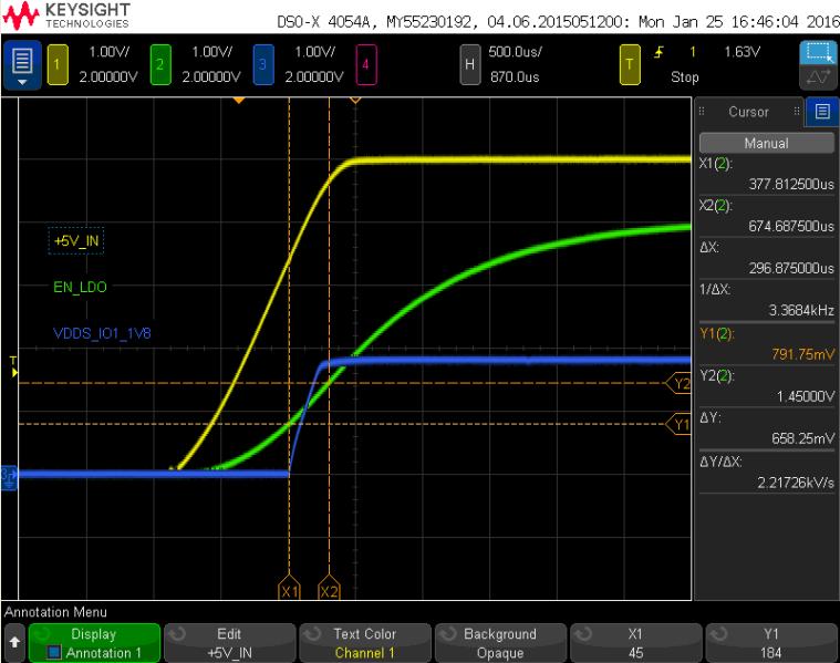
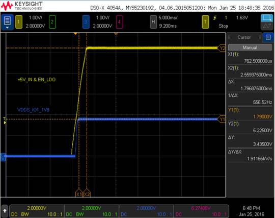
Why VDDS_IO1_1V8 stable time is faster than +5V_IN about 200uS?Is this a normal phenomenon?If yes, why?
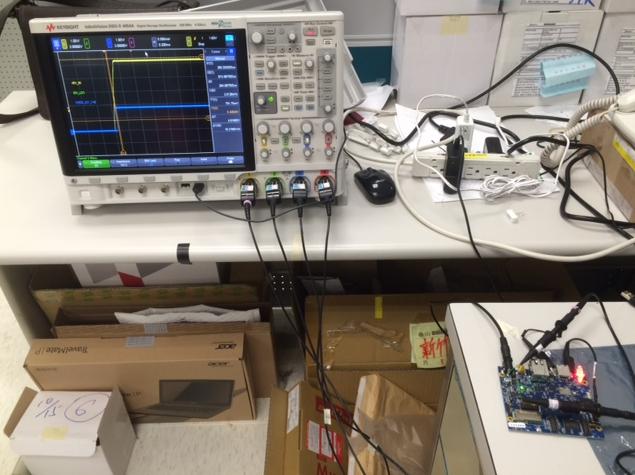
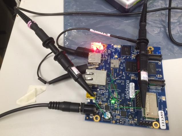
Below figures are EVM test result、test environment and schematic:
The EVM's EN_LDO and +5V_IN are connected together, so we compare output waveform with +5V_IN and LDO 1.8V.
After compared, the VDDS_IO1_1V8 stable time is faster than VDD_5V0 about 1.79mS,
and we found that the VDD_IO1_1V8 will be stable when +5V_VIN is about at 2.5V.
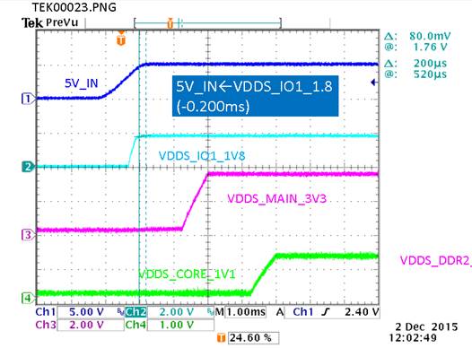
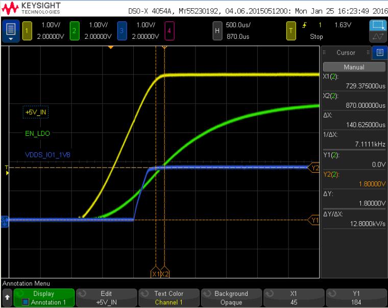
Then we measured it again on our board and you can refer to below schematic(SCHEMATIC1 _ 07 - CPU PMIC),
EN_LDO and +5V_IN are not connected together so we used two prob respectively for those two power.
And we found that the VDDS_IO1_1V8 stable time is faster than +5V_IN about 140.6uS.
SCHEMATIC1 _ 07 - CPU PMIC.pdf
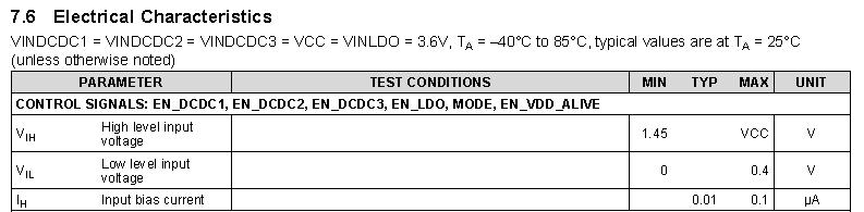
We've checked the spec of TPS650250 and its VIH/MIN is 1.45V、VIL/MAX is 0.4V as below table:
The VDDS_IO1_1V8 is powered on at 791.75mV, should we need to let EN_LDO input voltage lower than VIL 0.4V for complete turn it off?