This thread has been locked.

If you have a related question, please click the "Ask a related question" button in the top right corner. The newly created question will be automatically linked to this question.

LP2985-N Vout rising waveform at tune on

Other Parts Discussed in Thread: LP2985

Hi,

I and customer have questions about Vout rising waveform at tune on.
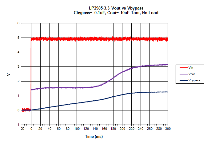
Vout waveform is showed at detasheet P21 Figure35~38.
Could you answer me the below questions, please?

Q1:Why does output voltage rise with stairs?
      Stairs means this.

Q2:My customer has a issue.
      Please see below picture.
      There is different of Vout waveform between Vin=12V and Vin=15.
      At this time, Bypass capacitor is same(0.01uF).
      Why does Vin=15V have large stairs voltage period?

Best regards,
Shimizu

  • Hi,

     I add information for Q2.

     Customer is using "GRM21BF111E225Z" as input capacitor.  

     This cap is subject to DC bias characteristics.

     Does this have a relationship?

    Best regards,

    Shimizu


  • The Vout waveform should always have some type of a step at start-up as this represents the Cbyp capacitor charging from 0V up to the reference voltage. The step will typically be just below 50% of the final Vout, and represents a cross-over point in the band-gap circuitry star-up that steals some current from the Cbyp current charge circuitry.
    Figure 35 would be for no Bypass capacitor (Cbyp= 0).
    If Bypass capacitor is 0.01uF, then Vout waveform should look closer to Figure 38 (Cbyp= 10nF).
  • I can not find any information for "GRM21BF111E225Z" at Digikey or Murata.

    A GOOGLE search for "GRM21BF111E225Z" returned:

         " Your search - GRM21BF111E225Z - did not match any documents. "

    My opinion is that Cin has no direct effect on the charging of Cbyp.

    Note that if the LP2985 powered-down and then restarted promptly, the step might be not be seen at the restart. This is because Cbyp pin does not have any dedicated discharge circuitry, so Cbyp hold the charge from the previous power-on. In effect, Cbyp is pre-charged.

  • Hi Donald,

     Thank you for your support.

     I mistook typing. GRM21BF11E225Z is right.

      "search.murata.co.jp/.../GRM21BF11C225ZA01-01.pdf"

     I'm sorry. this is Japanese document.

     At Page 15, It is showed DC bias characteristics.

     I think that Capacity at 12Vin and 15Vin is not satisfied capacity value of datasheet.


     And I add some questions(confirmation).

     Where does Cbyp start charging from?

     Please see below picture.

     T1 or T2?  


    Best regards,

    Shimizu

  • Ideally, Cbyp actually starts charging from 0V at T1.

    However, the band-gap start-up circuitry (and thus Vout)  stalls at T2 (approx 1 x Vbe) due to lack of sufficient current, while Cbyp continues to charge.

    At T3 the voltage on Cbyp is approx equal to 1 x Vbe, and the remainder of the Vout rise time is defined by Cbyp.

    Here is what it looks like with LP2985-3.3: