This thread has been locked.

If you have a related question, please click the "Ask a related question" button in the top right corner. The newly created question will be automatically linked to this question.

BQ76PL455A ADC issue

Other Parts Discussed in Thread: BQ76PL455A

Dear ..

I use stacked two bq76PL455A to make 32S battery pack.

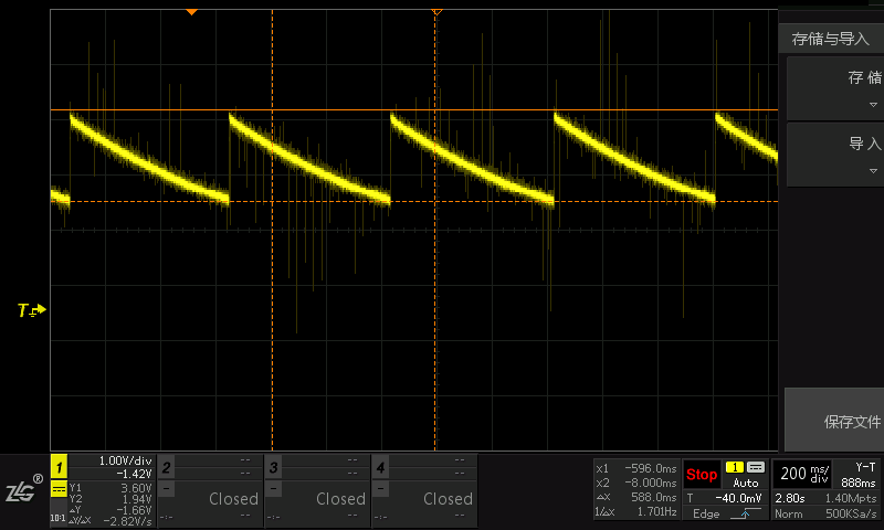
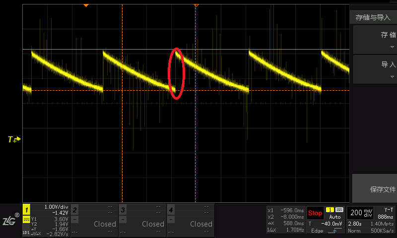
I'm going to read all of the battery voltage in every 200 ms, But I would occur voltage error data.  

The following is the wrong data.  

current = The current read data, last = last time read date , diff = The difference between two Numbers

CV diff:P0 M1 C4. current:2594,last:3825,diff:-1231.debonce:3825.Cnt:2.

CV diff:P0 M1 C5. current:2336,last:3825,diff:-1489.debonce:3825.Cnt:2.

CV diff:P0 M1 C6. current:2414,last:3824,diff:-1410.debonce:3824.Cnt:2.

CV diff:P0 M1 C7. current:2375,last:3825,diff:-1450.debonce:3825.Cnt:2.

CV diff:P0 M1 C8. current:2316,last:3824,diff:-1508.debonce:3824.Cnt:2.

CV diff:P0 M1 C9. current:2258,last:3824,diff:-1566.debonce:3824.Cnt:2.

CV diff:P0 M1 C10. current:2258,last:3824,diff:-1566.debonce:3824.Cnt:2.

CV diff:P0 M1 C11. current:2472,last:3824,diff:-1352.debonce:3824.Cnt:2.

CV diff:P0 M1 C12. current:2316,last:3824,diff:-1508.debonce:3824.Cnt:2.

CV diff:P0 M1 C13. current:2472,last:3824,diff:-1352.debonce:3824.Cnt:2.

CV diff:P0 M1 C14. current:2551,last:3825,diff:-1274.debonce:3825.Cnt:2.

CV diff:P0 M1 C15. current:11,last:3826,diff:-3815.debonce:3826.Cnt:2.

This is the configuration data.

Device Version(0x00:Digital die version number):8.

Device Version(0x01:Analog die version number):6.

CHANNELS 0x03-06 (3-6) Channel Select:ff.ff.3f.0

OVERSMPL 0x07 (7) Command Oversampling:fb.

ADDR 0x0A (10) Device Address:0.

GROUP_ID 0x0B

TXHOLDOFF 0x12 (18) UART Transmitter Holdoff:0.

CBCONFIG 0x13 (19) Balance Configuration:0.

CBENBL 0x14–15 (20-21) Balancing Enable:0-0.

TSTCONFIG 0x1E-1F (30-31) Test Configuration:0-0.

TESTCTRL 0x20-21 (32-33) Test Control:0-0.

TEST_ADC 0x22-24 (34-36) ADC Output Test:0-0-0.

CTO 0x28 (40) Communication Timeout:76.

CTO_CNT 0x29-2B (41-43) Communication Timeout Counter:0-0-1.

AM_PER 0x32 (50) Auto-Monitor Period:0.

AM_CHAN 0x33-36 (51-54) Auto-Monitor Channel Select:0-0-0-0.

AM_OSMPL 0x37 (55) Auto-Monitor Oversampling:0.

SMPL_SLY1 0x3D (61) Initial Sampling Delay:0.

Cell_CSPER 0x3E (62) Cell Voltage and Internal Temperature Sampling Interval:ec.

AUX_SPER 0x3F-42 (63-66) AUX Sampling Period:0-0-0-0.

TEST_SPER 0x43-44 (67-68) Test Sampling Periods:f9-99.

SHDN_STS 0x50 (80) Shutdown Recovery Status:80.

STATUS 0x51 (81) Device Status:0.

FAULT_SUM 0x52-53 (82-83) Fault Summary:0-0.

FAULT_COM 0x5E-5F (94-95) Communications Fault:0-0.

FAULT_SYS 0x60 (96) System Fault:0.

FAULT_DEV 0x61-62 (97-98) Chip Fault:0-0.

FAULT_GPI 0x63 (99) GPI Fault:0.

FO_CTRL 0x6E-6F (110-111) Fault Output Control:0-0.

LOT_NUM 0xBE-C5 (190-197) Device Lot Number:f-52.

SER_NUM 0xC6-C7 (198-199) Device Serial Number:b-4d.

TSTR_ECC 0xE6-ED (230-237) ECC Test Result[1:0]:0-0-0-0.

CSUM 0xF0-F3 (240-243) Checksum:fd-1d-88-2f.

CSUM_RSLT 0xF4-F7(244-247) Checksum Readout:fd-1d-88-2f.

TEST_CSUM 0xF8-F9 (248-249) Checksum Test Result:0-0.

EE_BURN 0xFA (250) EEPROM Burn Count:2.

  • I tried with your setting and I have no issues with cell measurements.

    What caps do you have on OUT?

    or, can I take a quick review on your schematic?


    0

    Gerbo Version

    R

    1

    N

    08


    1

    Hulk Version

    R

    1

    N

    06


    2

    Command

    W

    1

    N

    00


    3

    Command Channel Select

    RW

    4

    Y

    FFFF3F00


    7

    Command Oversampling

    RW

    1

    Y

    FB


    10

    Device Address

    RW

    1

    Y

    00


    11

    Group ID

    RW

    1

    Y

    00


    12

    Device Control

    RW

    1

    N

    00


    13

    Number Channels

    RW

    1

    Y

    10


    14

    Device Configuration

    RW

    1

    Y

    10


    15

    Power Configuration

    RW

    1

    Y

    80


    16

    Communication Configuration

    RW

    2

    Y

    1080


    18

    UART Transmitter Holdoff

    RW

    1

    Y

    00


    19

    Balance Configuration

    RW

    1

    Y

    00


    20

    Balancing Enable

    RW

    2

    N

    0000


    30

    Test Configuration

    RW

    2

    N

    0000


    32

    Test Control

    RW

    2

    N

    0000


    34

    ADC Output Test

    RW

    3

    N

    000000


    37

    AUX Pullup Test Control

    RW

    1

    N

    00


    40

    Communication Timeout

    RW

    1

    Y

    DC


    41

    Communication Timeout Counter

    RW

    3

    N

    000001


    50

    Auto-Monitor Period

    RW

    1

    Y

    00


    51

    Auto-Monitor Channel Select

    RW

    4

    Y

    00000000


    55

    Auto-Monitor Oversampling

    RW

    1

    Y

    00


    61

    Initial Sampling Delay

    RW

    1

    Y

    00


    62

    Voltage & Internal Temp Sampling Period

    RW

    1

    Y

    EC


    63

    AUX Sampling Period

    RW

    4

    Y

    44444444


    67

    Test Sampling Periods

    RW

    2

    Y

    F999


    80

    Shutdown Recovery Status

    R

    1

    N

    80


    81

    System Status

    RW

    1

    N

    00


    82

    Fault Summary

    RW

    2

    N

    0000


    84

    Cell Under-Voltage Fault

    RW

    2

    N

    0000


    86

    Cell Over-Voltage Fault

    RW

    2

    N

    0000


    88

    Auxiliary Under/Over-Threshold Fault

    RW

    2

    N

    0000


    90

    Comparator Under-Voltage Fault

    RW

    2

    N

    0000


    92

    Comparator Over-Voltage Fault

    RW

    2

    N

    0000


    94

    Communication Fault

    RW

    2

    N

    0000


    96

    System Fault

    RW

    1

    N

    00


    97

    Device Fault

    RW

    2

    N

    0000


    99

    GPI Fault

    RW

    1

    N

    00


    104

    Communication Fault Masks

    RW

    2

    Y

    0000


    106

    System Fault Masks

    RW

    1

    Y

    10


    107

    Device Fault Masks

    RW

    2

    Y

    0000


    110

    Fault Output Control

    RW

    2

    Y

    FFC0


    120

    General Purpose IO Direction

    RW

    1

    Y

    00


    121

    General Purpose Output

    RW

    1

    Y

    00


    122

    General Purpose Pullup

    RW

    1

    Y

    00


    123

    General Purpose Pulldown

    RW

    1

    Y

    00


    124

    General Purpose Input

    R

    1

    N

    00


    125

    General Purpose Fault Input

    RW

    1

    Y

    00


    130

    Magic1

    W

    4

    N

    00000000


    140

    Comparator Under-Voltage Threshold

    RW

    1

    Y

    00


    141

    Comparator Over-Voltage Threshold

    RW

    1

    Y

    FE


    142

    Cell Under-Voltage Threshold

    RW

    2

    Y

    0000


    144

    Cell Over-Voltage Threshold

    RW

    2

    Y

    FFFC


    146

    AUX0 Under-Voltage Threshold

    RW

    2

    Y

    0000


    148

    AUX0 Over-Voltage Threshold

    RW

    2

    Y

    FFFC


    150

    AUX1 Under-Voltage Threshold

    RW

    2

    Y

    0000


    152

    AUX1 Over-Voltage Threshold

    RW

    2

    Y

    FFFC


    154

    AUX2 Under-Voltage Threshold

    RW

    2

    Y

    0000


    156

    AUX2 Over-Voltage Threshold

    RW

    2

    Y

    FFFC


    158

    AUX3 Under-Voltage Threshold

    RW

    2

    Y

    0000


    160

    AUX3 Over-Voltage Threshold

    RW

    2

    Y

    FFFC


    162

    AUX4 Under-Voltage Threshold

    RW

    2

    Y

    0000


    164

    AUX4 Over-Voltage Threshold

    RW

    2

    Y

    FFFC


    166

    AUX5 Under-Voltage Threshold

    RW

    2

    Y

    0000


    168

    AUX5 Over-Voltage Threshold

    RW

    2

    Y

    FFFC


    170

    AUX6 Under-Voltage Threshold

    RW

    2

    Y

    0000


    172

    AUX6 Over-Voltage Threshold

    RW

    2

    Y

    FFFC


    174

    AUX7 Under-Voltage Threshold

    RW

    2

    Y

    0000


    176

    AUX7 Over-Voltage Threshold

    RW

    2

    Y

    FFFC


    190

    Device Lot Number

    R

    8

    N

    0F58D18C196DC40F


    198

    Device Serial Number

    R

    2

    N

    019C


    200

    Customer Scratchpad

    RW

    8

    Y

    0000000000000000


    210

    Customer Cell Offset

    RW

    1

    Y

    00


    211

    Customer Gain Offset

    RW

    1

    Y

    00


    212

    Customer AUX0 Offset

    RW

    2

    Y

    0000


    214

    Customer AUX1 Offset

    RW

    2

    Y

    0000


    216

    Customer AUX2 Offset

    RW

    2

    Y

    0000


    218

    Customer AUX3 Offset

    RW

    2

    Y

    0000


    220

    Customer AUX4 Offset

    RW

    2

    Y

    0000


    222

    Customer AUX5 Offset

    RW

    2

    Y

    0000


    224

    Customer AUX6 Offset

    RW

    2

    Y

    0000


    226

    Customer AUX7 Offset

    RW

    2

    Y

    0000


    230

    ECC Test Result

    R

    8

    N

    0000000000000000


    240

    Customer Checksum

    RW

    4

    Y

    C9EF5377


    244

    Customer Checksum Readout

    R

    4

    N

    C9EF5377


    248

    Checksum Test Result

    R

    2

    N

    0000


    250

    EEPROM Burn Count

    RW

    1

    Y

    00


    252

    Magic2

    W

    4

    N

    00000000

  • @Roger Hwang ,   I have the same issue like that: The cell voltage would change very large sometimes.

    The registers setting  list  as flow:

    Device Version 0x00 (0) Digital die version number):8.

    Device Version 0x01 (1) Analog die version number):6.

    CHANNELS 0x03-06 (3-6) Channel Select:ff.ff.3f.0

    OVERSMPL 0x07 (7) Command Oversampling:7b.

    ADDR 0x0A (10) Device Address:0.

    GROUP_ID 0x0B (11) Group ID:0.

    DEV_CTRL 0x0C (12) Device Control:0.

    NCHAN 0x0D (13) Number of Channels:10.

    DEVCONFIG 0x0E (14) Device Configuration:10.

    PWRCONFIG (0x0F) (15) Power Configuration:80.

    COMCONFIG 0x10-11 (16-17) Communications Configuration:10-c0.

    TXHOLDOFF 0x12 (18) UART Transmitter Holdoff:0.

    CBCONFIG 0x13 (19) Balance Configuration:0.

    CBENBL 0x14–15 (20-21) Balancing Enable:0-0.

    TTSTCONFIG 0x1E-1F (30-31) Test Configuration:0-0.

    TESTCTRL 0x20-21 (32-33) Test Control:0-0.

    TEST_ADC 0x22-24 (34-36) ADC Output Test:0-0-0-0.

    CTO 0x28 (40) Communication Timeout:76.

    CTO_CNT 0x29-2B (41-43) Communication Timeout Counter::0-0-1-0.

    AM_PER 0x32 (50) Auto-Monitor Period:0.

    AM_CHAN 0x33-36 (51-54) Auto-Monitor Channel Select:0-0-0-0

    AM_OSMPL 0x37 (55) Auto-Monitor Oversampling:0.

    SMPL_SLY1 0x3D (61) Initial Sampling Delay:0.

    Cell_CSPER 0x3E (62) Cell Voltage and Internal Temperature Sampling Interval:bc.

    AUX_SPER 0x3F-42 (63-66) AUX Sampling Period:44.44.44.44

    TEST_SPER 0x43-44 (67-68) Test Sampling Periods:f9.99

    SHDN_STS 0x50 (80) Shutdown Recovery Status:80.

    STATUS 0x51 (81) Device Status:0.

    FAULT_SUM 0x52-53 (82-83) Fault Summary:0.0

    FAULT_COM 0x5E-5F (94-95) Communications Fault:0.0

    FAULT_SYS 0x60 (96) System Fault:0.

    FAULT_DEV 0x61-62 (97-98) Chip Fault:0.0

    FAULT_GPI 0x63 (99) GPI Fault:0.

    FO_CTRL 0x6E-6F (110-111) Fault Output Control:0.0

    LOT_NUM 0xBE-C5 (190-197) Device Lot Number: f.52.56.15.17.43.53.f

    SER_NUM 0xC6-C7 (198-199) Device Serial Number:6.b2

    TSTR_ECC 0xE6-ED (230-237) ECC Test Result[1:0]: 0.0.0.0.0.0.0.0

    CSUM 0xF0-F3 (240-243) Checksum: 64.2e.13.37

    CSUM_RSLT 0xF4-F7(244-247) Checksum Readout : 64.2e.13.37

    TEST_CSUM 0xF8-F9 (248-249) Checksum Test Result: 0.0.2.0

    EE_BURN 0xFA (250) EEPROM Burn Count:2.

    The caps  on OUT value 100nF; and the scope is

    Could you give me some suggest?

    Thanks!

  • @Roger Hwang , I have the same issue like that.

    The registers setting list as flow:
    Device Version 0x00 (0) Digital die version number):8.
    Device Version 0x01 (1) Analog die version number):6.
    CHANNELS 0x03-06 (3-6) Channel Select:ff.ff.3f.0
    OVERSMPL 0x07 (7) Command Oversampling:7b.
    ADDR 0x0A (10) Device Address:0.
    GROUP_ID 0x0B (11) Group ID:0.
    DEV_CTRL 0x0C (12) Device Control:0.
    NCHAN 0x0D (13) Number of Channels:10.
    DEVCONFIG 0x0E (14) Device Configuration:10.
    PWRCONFIG (0x0F) (15) Power Configuration:80.
    COMCONFIG 0x10-11 (16-17) Communications Configuration:10-c0.
    TXHOLDOFF 0x12 (18) UART Transmitter Holdoff:0.
    CBCONFIG 0x13 (19) Balance Configuration:0.
    CBENBL 0x14–15 (20-21) Balancing Enable:0-0.
    TTSTCONFIG 0x1E-1F (30-31) Test Configuration:0-0.
    TESTCTRL 0x20-21 (32-33) Test Control:0-0.
    TEST_ADC 0x22-24 (34-36) ADC Output Test:0-0-0-0.
    CTO 0x28 (40) Communication Timeout:76.
    CTO_CNT 0x29-2B (41-43) Communication Timeout Counter::0-0-1-0.
    AM_PER 0x32 (50) Auto-Monitor Period:0.
    AM_CHAN 0x33-36 (51-54) Auto-Monitor Channel Select:0-0-0-0
    AM_OSMPL 0x37 (55) Auto-Monitor Oversampling:0.
    SMPL_SLY1 0x3D (61) Initial Sampling Delay:0.
    Cell_CSPER 0x3E (62) Cell Voltage and Internal Temperature Sampling Interval:bc.
    AUX_SPER 0x3F-42 (63-66) AUX Sampling Period:44.44.44.44
    TEST_SPER 0x43-44 (67-68) Test Sampling Periods:f9.99
    SHDN_STS 0x50 (80) Shutdown Recovery Status:80.
    STATUS 0x51 (81) Device Status:0.
    FAULT_SUM 0x52-53 (82-83) Fault Summary:0.0
    FAULT_COM 0x5E-5F (94-95) Communications Fault:0.0
    FAULT_SYS 0x60 (96) System Fault:0.
    FAULT_DEV 0x61-62 (97-98) Chip Fault:0.0
    FAULT_GPI 0x63 (99) GPI Fault:0.
    FO_CTRL 0x6E-6F (110-111) Fault Output Control:0.0
    LOT_NUM 0xBE-C5 (190-197) Device Lot Number: f.52.56.15.17.43.53.f
    SER_NUM 0xC6-C7 (198-199) Device Serial Number:6.b2
    TSTR_ECC 0xE6-ED (230-237) ECC Test Result[1:0]: 0.0.0.0.0.0.0.0
    CSUM 0xF0-F3 (240-243) Checksum: 64.2e.13.37
    CSUM_RSLT 0xF4-F7(244-247) Checksum Readout : 64.2e.13.37
    TEST_CSUM 0xF8-F9 (248-249) Checksum Test Result: 0.0.2.0
    EE_BURN 0xFA (250) EEPROM Burn Count:2.


    The caps on OUT value 100nF;
  • @Roger Hwang , I have the same issue like that: The cell voltage would change very large sometimes.


    The registers setting list as flow:

    Device Version 0x00 (0) Digital die version number):8.

    Device Version 0x01 (1) Analog die version number):6.

    CHANNELS 0x03-06 (3-6) Channel Select:ff.ff.3f.0

    OVERSMPL 0x07 (7) Command Oversampling:7b.

    ADDR 0x0A (10) Device Address:0.

    GROUP_ID 0x0B (11) Group ID:0.

    DEV_CTRL 0x0C (12) Device Control:0.

    NCHAN 0x0D (13) Number of Channels:10.

    DEVCONFIG 0x0E (14) Device Configuration:10.

    PWRCONFIG (0x0F) (15) Power Configuration:80.

    COMCONFIG 0x10-11 (16-17) Communications Configuration:10-c0.

    TXHOLDOFF 0x12 (18) UART Transmitter Holdoff:0.

    CBCONFIG 0x13 (19) Balance Configuration:0.

    CBENBL 0x14–15 (20-21) Balancing Enable:0-0.

    TTSTCONFIG 0x1E-1F (30-31) Test Configuration:0-0.

    TESTCTRL 0x20-21 (32-33) Test Control:0-0.

    TEST_ADC 0x22-24 (34-36) ADC Output Test:0-0-0-0.

    CTO 0x28 (40) Communication Timeout:76.

    CTO_CNT 0x29-2B (41-43) Communication Timeout Counter::0-0-1-0.

    AM_PER 0x32 (50) Auto-Monitor Period:0.

    AM_CHAN 0x33-36 (51-54) Auto-Monitor Channel Select:0-0-0-0

    AM_OSMPL 0x37 (55) Auto-Monitor Oversampling:0.

    SMPL_SLY1 0x3D (61) Initial Sampling Delay:0.

    Cell_CSPER 0x3E (62) Cell Voltage and Internal Temperature Sampling Interval:bc.

    AUX_SPER 0x3F-42 (63-66) AUX Sampling Period:44.44.44.44

    TEST_SPER 0x43-44 (67-68) Test Sampling Periods:f9.99

    SHDN_STS 0x50 (80) Shutdown Recovery Status:80.

    STATUS 0x51 (81) Device Status:0.

    FAULT_SUM 0x52-53 (82-83) Fault Summary:0.0

    FAULT_COM 0x5E-5F (94-95) Communications Fault:0.0

    FAULT_SYS 0x60 (96) System Fault:0.

    FAULT_DEV 0x61-62 (97-98) Chip Fault:0.0

    FAULT_GPI 0x63 (99) GPI Fault:0.

    FO_CTRL 0x6E-6F (110-111) Fault Output Control:0.0

    LOT_NUM 0xBE-C5 (190-197) Device Lot Number: f.52.56.15.17.43.53.f

    SER_NUM 0xC6-C7 (198-199) Device Serial Number:6.b2

    TSTR_ECC 0xE6-ED (230-237) ECC Test Result[1:0]: 0.0.0.0.0.0.0.0

    CSUM 0xF0-F3 (240-243) Checksum: 64.2e.13.37

    CSUM_RSLT 0xF4-F7(244-247) Checksum Readout : 64.2e.13.37

    TEST_CSUM 0xF8-F9 (248-249) Checksum Test Result: 0.0.2.0

    EE_BURN 0xFA (250) EEPROM Burn Count:2.

    The caps on OUT value 100nF; and the scope is


    Could you give me some suggest?

    Thanks!
  • HI PinKen,

    We recommend 390pF on OUT filter Cap.

    The recommended sample configuration settings are (these are also the factory default):

    You can also find them in the datasheet table 3.

    -        390pF OUT filter cap

    -        AFE_PCTRL = 1 (causes 100us for ADC power up)

    -        Cell ADC sample period (ADC_PERIOD_VOL) = 60us

    -        Cell ADC sample period for oversamples (CMD_OVS_GPER) = 12.6us

    -        Staying on a cell channel to oversample (CMD_OVS_CYCLE)

    -        AUX ADC sample period = 12.6us (ADC_PERIOD_AUXx)

    -        8x oversampling of CELL and AUX channels (CMD_OVSMP)

    -        All of these parameters would be applied to any channels being sampled, including AUX, etc.


    These are factory default value and GAIN and OFFSET are all calibrate with these settings.

    Can you change CAP to 390pF and follow our register settings?

    Is there concern for not following our recommendation? 

    Please follow our recommendations and let us know if you still have any problems.

  • As Roger mentioned, 

    The recommended sample configuration settings are (these are also the factory default):

    -          390pF OUT filter cap

    -          AFE_PCTRL = 1 (causes 100us for ADC power up)

    -          Cell ADC sample period (ADC_PERIOD_VOL) = 60us

    -          Cell ADC sample period for oversamples (CMD_OVS_GPER) = 12.6us

    -          Staying on a cell channel to oversample (CMD_OVS_CYCLE)

    -          AUX ADC sample period = 12.6us (ADC_PERIOD_AUXx)

    -          8x oversampling of CELL and AUX channels (CMD_OVSMP)

    -          All of these parameters would be applied to any channels being sampled, including AUX, etc.


    You appear to be using the following settings which deviate from our recommendations:

    -          CMD_OVS_CYCLE = 1 (cycle through all channels one at a time)

    -          Cell ADC sample period (ADC_PERIOD_VOL) = 500us

    -          AUX ADC sample period for oversamples (CMD_OVS_GPER) = 5.96us


    These settings together with a 100nF OUT cap have not been tested. I suspect OUT cap value is far too large. We can only support the ADC configuration in the recommendations above used with a 390pF OUT cap. Any changes from those settings will need to be characterized by the customer to determine if it is a good combination.

    I suggest monitoring the OUT pin with a differential probe to determine there is enough time for the AFE MUX output voltage to settle before the ADC samples. If the MUX output has not settled in time, then the cap value will need to be decreased. Your oscilloscope capture of the OUT signal needs to be zoomed in much more in the area shown below:

  • The OUT signal (when zoomed in) should look like this:

    The zoomed in view of the OUT signal in the bottom half of the capture shows the MUX output changing from cell 16 to cell 15. The dip is the MUX output settling. It must be given sufficient time to settle before sampling occurs (right before the MUX output changes to the next channel). With too big of a cap value, the MUX output may still be changing when the sampling occurs.