This thread has been locked.

If you have a related question, please click the "Ask a related question" button in the top right corner. The newly created question will be automatically linked to this question.

TPS63000DRCRG4 is defect and getting hot after a long time of operation

Other Parts Discussed in Thread: TPS63000

Hello,

We have this problems with one particular batch of TPS63000 IC's. They are used in a buck/boost configuration, to convert an input voltage of 3.6 Volts , lithium battery, into a regulated 3.6 Volts supply voltage.

The devices have worked for approx one year, and now they are defect. The symptom is that the IC gets very hot, and it is oscillating at a very low frequency (21 Hz), with a high frequency component on it (high level). It is generating approx 3 Volts.  It is drawing way too much current from the battery.

It seems that this problem is related to a certain batch of IC's, because we never had this problem before, and Now we see this happening with IC from one batch.

can anyone help?

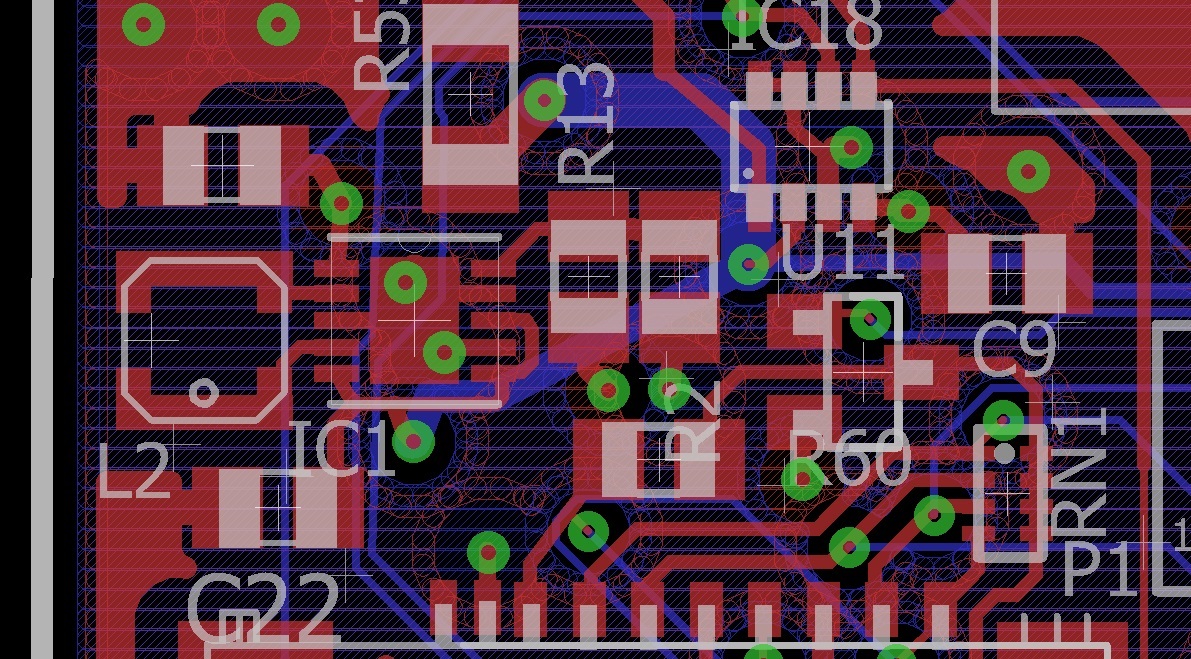
  • Can you please post the schematic and the layout.
    I want to clarify something. Does the same IC get hotter after working for one year? Or do you see this issue as soon as you solder a new IC "from this batch" on your board?
  • Hello,

    We have this problem after one year of normal operation. We had it fout times now. And all were from one batch.

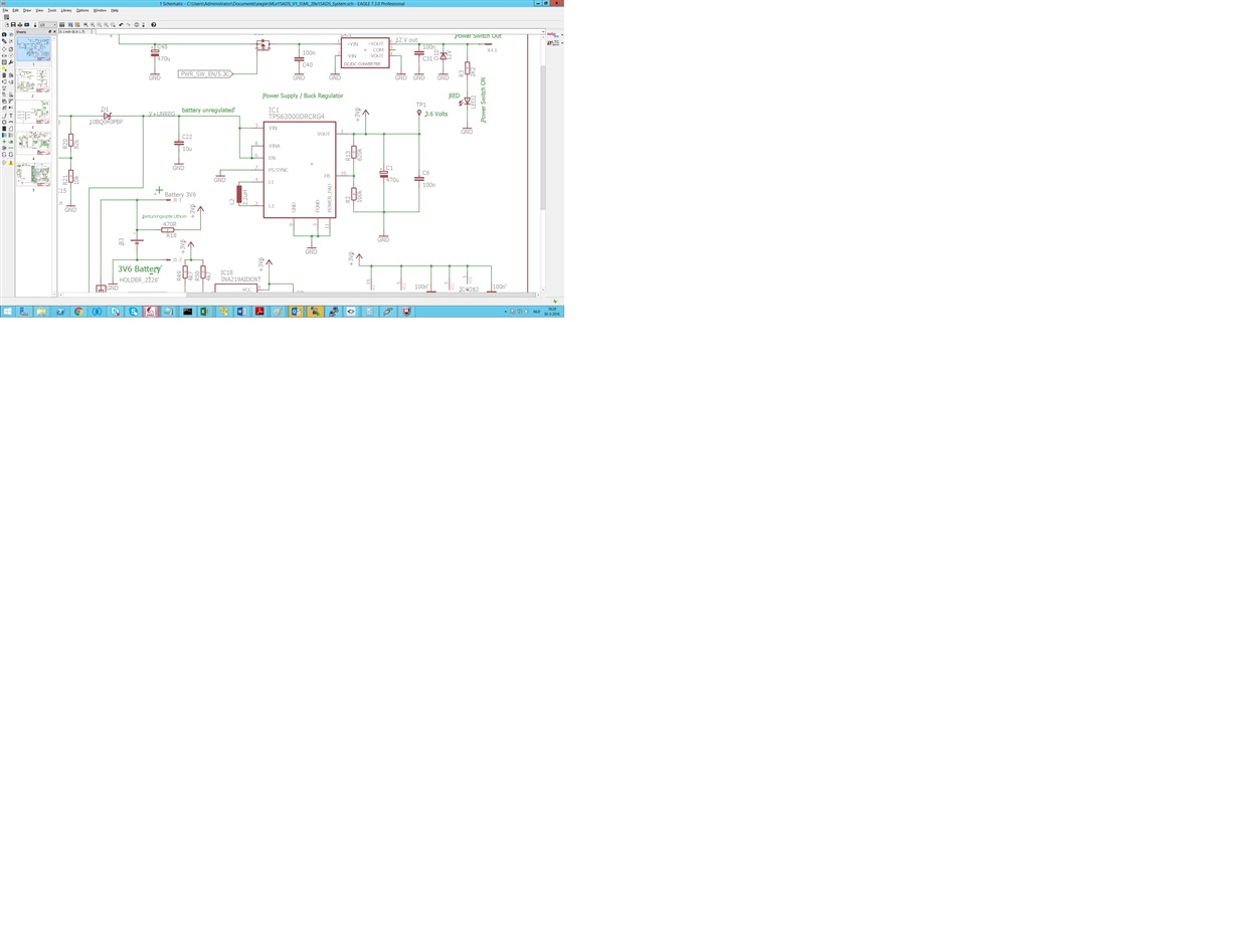
    This is the schematics:

     The board is a 4 layer board with one layer of gnd and one layer of vdd. The IC has two via's to gnd, for cooling. But the device (a datalogger ) is very low power, so heat is not the problem.

    :

  • Update: I discovered that the output of the device gets a ripple when the input voltage gets above 4.4 Volts. Below that value it works fine.
    Also I mention that, when the load is very low, there is a very low frequency ripple (>10 sec). I understand, because the load is below 50uA, and with only a little energy, the voltage is above the setpoint. The input voltage gets "peaks"on it when the inputvoltage gets above 4.4 Volts. I also was able to check the voltage when 2 of the devices went defect: 4.5 Volts (this voltage was automatically stored and just before the device broke) So, above 4.4 Volts: output ripple and input voltage spikes. Below 4.4 Volts all ok.
  • I am actually  surprised that the device worked for one year with this layout.

    The input and output capacitors are placed far from the IC and are connected with small traces, this adds parasitic inductance and reduces the actual effective capacitance the IC sees. The ground connection of these capacitors is also not optimal, they are way too long. Moreover the power pad of the IC has only two vias which is not sufficient.

    The kind of behavior you describe in your "update" is is strongly linked to poor layout. To have a reliable design I would definitely change the layout, and follow the layout recommendation of the datasheet.

    The layout is one of the most critical part of the design, and with this actual layout you can not get reliable performances out of the device. Never hesitate to send the schematic and layout for reviewing before going into production.