This thread has been locked.

If you have a related question, please click the "Ask a related question" button in the top right corner. The newly created question will be automatically linked to this question.

TPS65150 VGH not smooth but a sawtooth waveform

Other Parts Discussed in Thread: TPS65150

Hello,

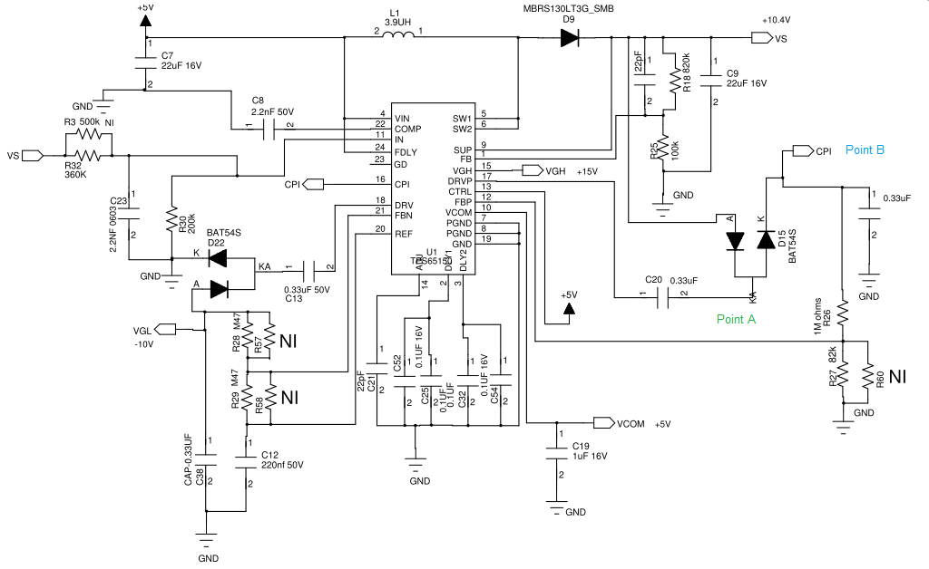
I am using the TPS65150 following the typical application circuit in the datasheet.  I only have problem with VGH

VS = 10.4V OK

VGH = 16 V , desired   ,  design values for R5=1M, R6=82K   --> this resulted in a much higher peaks that is not good for LCD.

 currently using R5=1M,  R6= 87.5K,  C4=C16=0.33uF.

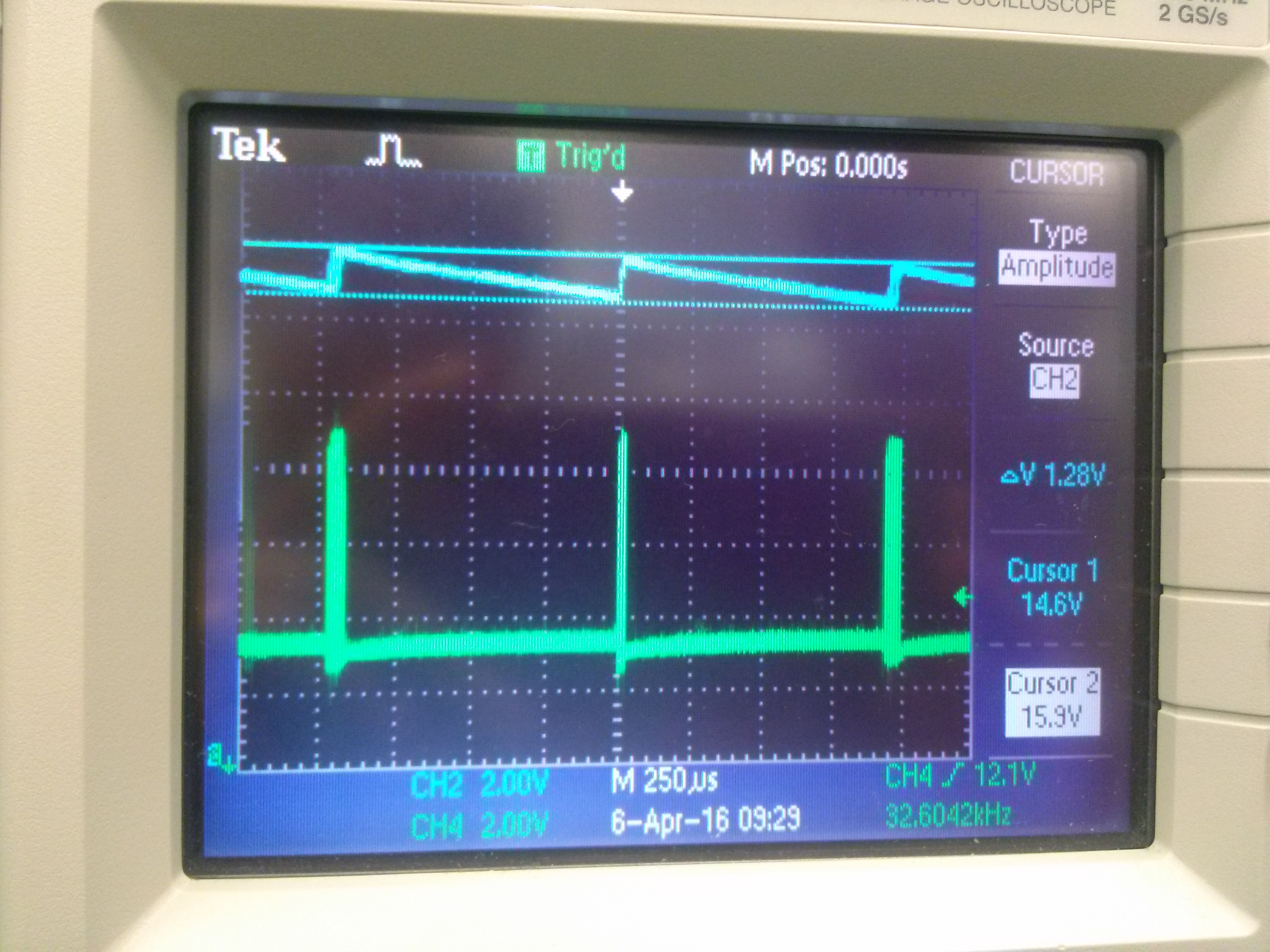
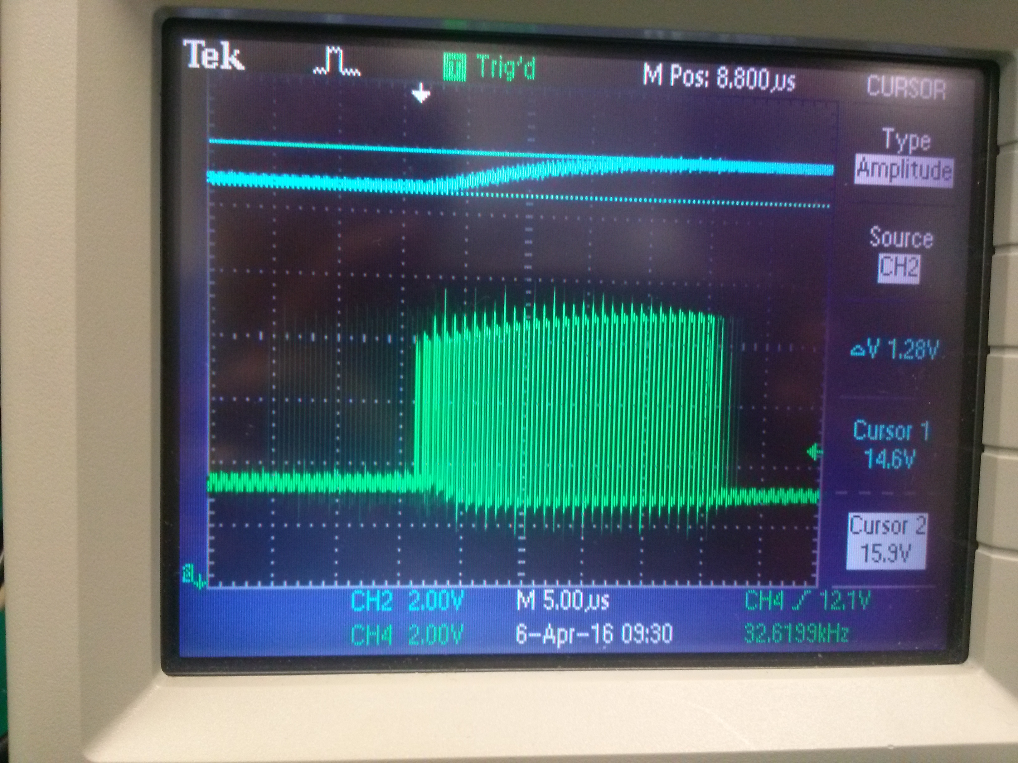
The CPI output is a sawtooth peak = 17V , trough = 15.8V,   LCD is not stable.

I measuring the ANODE of D5 I can see burst of 1.2Mhz pulse when that creates the 17V peaks of the sawtooth output, following by no pulses and the output drops to about 15.8V and the burst comes in to raise the output back to 17V.


Is there a need to change C4 and/or C16?  There is no spec regarding the how much current that LCD needs.
Please help.


  • Please post a copy of your schematic.
    I would like to double-check that your circuit really is identical to the one in the data sheet.
  • Hello,


    Thank you for your response.  I have uploaded the portion of circuit and also some of the captured wave form.  Please note that the R27 is not 82K but 90K when the waveforms were captured.

    Blue wave taken at Point B,  the CPI output at the capacitor, see the sawtooth wave.

    Green wave taken at Point A, the burst of 1.2Mhz pulses that push up the CPI voltage, then followed by a period of no pulses.

    Please note CPI voltage of the circuit  using the formula given in the datasheet,

    Vo = Vref(1 + R1/R2) = 1.213*(1+ 1000/90)=14.7V.


    From the wave captured, CPI  Voltage is 14.6V and 15.9V.  It seems that the burst of pulse over charge the caps and pushed the output


    Increasing the capacitor at CPI only slightly reduce amplitude of the saw-tooth and lengthen the period of the saw-tooth.

    The LCD module (AT070TN92) I am working on needs a VS= 10.4V, VGL=-7V,  VGH=16V, VCOM=5.  All the voltages are OK except VGH. 

    The current for VGH was not given in the datasheets, but from other similarly spec device (AT070TN82) from the same company, the voltages VGL,VGH,AVDD are the same as that of the AT070TN92.  The indicated VGH of the AT070TN82 is 16V at IGH 0.2mA typical and 0.5mA Max, so I will take the assumption that the IGH is between 0.2mA and 0.5mA.  With this information, how do I go about designing the circuit to give the correct VGH=16V

    Are the exact values for C20 or Cfly critcal? How to calculate the correct value of C20 (my schematic) or Cfly (datasheet)?


    Please help exactly what needs to be changed to get a smooth CPI / VGH output?  A CPI with such large ripple (1.3V) is not acceptable.

    Thanks.


  • Hello,

    Thank you for your response,  I had posted a reply with my circuit and some captured waveform.
     but it did not appear so now I post again.

    The datasheet of AT070TN92  did not specify the current requirement for VGH.  but looking at a similar device AT070TN82 it appears that VGH requires typically 0.2mA and to a max of 0.5mA.  

    Please note that the R27 is not 82K but 90K when the waveforms are captured.  I guess is that C20 (Cfly) and/or Coutput at the CPI must be changed.  Is there any recommended design procedure for calculating Cfly.  Co calculation given in the datasheet don't seem to hold as you can see the large ripple at the CPI (Blue).  I think a reduction in the value of C20/Cfly from the given 0.33uf may be needed to smooth out the ripple.

    Please help.

  • The behavior you describe and what your scope plots show is not normal output voltage ripple, so I don't recommend you change any capacitor values. As you say, the positive charge pump switches for a few cycles, and then stops, presumably because the voltage on the FBP pin tells it the output is too high.

    It's possible that the positive charge pump in the TPS65150 is damaged, so I would recommend replacing U1. Your circuit looks fine to me; it's almost identical to the circuit used in our Evaluation Modules, which we know work correctly with these component values.

    Please try your circuit with a new TPS65150 and let me know how you get on.
  • Hello TI,


    Thank you for your reply,  and the suggestion of a damaged TPS65150.  I have about 50 prototype units with the said circuit.

    I have tested more than 12 of them, and they all showed the same kind of waveform.  I don't know what to make of it.  We did not use a scope to "see" VGH during our very first evaluation.Recently the QA department rejected the LCD displays as some very faint scrolling bars can  be seen upon close observations that prompted we started checking all the signals.  

    I am doubtful that I had a bad TPS65150.  Are we so bad luck that all the TPS65150s are bad?  

    I don't want take drastic measures redesigning the whole LCD bias voltage section.  Let's work on the problem further and see whether we can continue using the TPS65150.   We are using the TPS65150 in multiple LCD projects, getting to the bottom of the problem is crucial to give us the confident that the TPS65150 is really able to do the job.

    To continue discussion, you could give me more information to work with, for example :

    The load current of my LCD at VGH is less than 1mA, but the typical application design was for 20mA, are you certain it will work in my case?  I suspect that 0.5mA load is too small for the design to handle properly.

    How do you calculate and select those values of the components for the VGH section in the evaluation board (www.ti.com/.../slvuag5a.pdf) Cfly, Co etc,

    What are the expected waveform at various points in the circuit?  Can you post some pics?

    What is the expected voltage at FBP(R27)?  I was expecting 1.213V, but  the measured value was 1.02V. Is there something wrong here? The voltage at REF is 1.213V as expected.

    With different values of R27(my circuit), I can measure a different voltage at FBP,  is that perfectly OK?

    Because it is not 1.213V, the chosen values for R27 will not give the desired design Vcpi.  Can you explain what is going on?

    That is all I have to say.  Hope hear some insight information from you.

    Thanks.

  • I agree with you, if you have more than one circuit that shows this behavior, it is unlikely to be caused by a faulty/damaged TPS65150.

    I can't see anything wrong with your schematic, and I tested an EVM yesterday and I got 16 V from the positive charge pump with 330-nF capacitors, R27 = 82k, and no load connected. It worked just fine, so I suspect the problem may lie in the implementation of your circuit, not its design. At least, I think that's where we should focus our efforts right now.

    The FBP pin should be at 1.213 V, so something's not right there. Did you look at this pin with a scope, or just measure the voltage with a voltmeter? With the circuit unpowered, can you verify that there's a dc connection between the junction of R26 and R27 and the FBP pin?

    Can you please also tell me the exact part number of the flying and output capacitors, and send the PCB layout (pdf or Gerber format) to n-smith@ti.com.
  • Hi,

    The capacitor is this:
    www.mouser.sg/.../

    For the PCB layout, I need to get back to our PCB designer.
  • Your capacitor choice looks good.

    To test your charge pump, you can do the following:

    1) Disconnect the load from your charge pump.

    2) Apply a voltage greater than 1.213 V to the FBP pin and monitor the voltage on the DRVP pin. The charge pump should stop switching. This is my scope plot of the DRVP pin when I applied 1.220 V to the FBP pin.

    3) Apply a voltage less than 1.213 V to the FBP pin and monitor the voltage on the DRVP pin. The charge pump should switch with an amplitude of about 10 V (the voltage on its SUP pin). DOING THIS WILL FORCE YOUR VGH VOLTAGE TO ABOUT 21 V – MAKE SURE NOTHING IS CONNECTED THAT WILL GET DAMAGED BY THIS VOLTAGE LEVEL. This is my scope plot of the DRVP pin when I applied 1.200 V to the FBP pin.

    Your capacitor choice looks good.


    What load do you have connected to VGH when you make your measurements? Do you get the same voltage ripple on VGH if you disconnect the display?

  • Hi Nigel,


    Thank you for your post.  Your post prompted me to look into another model of LCD display we had that also use the 65150.  I measured VGH for this model and it was perfectly smooth.   Checking DRVP, I noticed that the VGH is actually doing its job and maintain VGH stable and flat.

    Whereas in the problematic model that we were talking about, as you can see from the waveform I sent earlier, the 65150 did tried to regulate the VGH but overshot the desired value.  I figured it might be some noise/ringing due to the PCB layout that affected FBP sensing the voltage correctly.  So I added a 33pf across the FBP and GND.  Now the VGH is smooth. 

    What do you think?  Is that a possible workaround to problem?  I hope you might provide me with some expert explanation as to why what I did worked. 

    Thanks.

  • Aha! That's good progress :-)

    The most important next step is to understand which signals are coupling into the FBP pin and causing the problem, and which part of the PCB layout is causing that. It's important that the root cause of the problem is fully understood before designating it as fixed. I've "fixed" many circuits by adding a capacitor somewhere, only later to find that the additional capacitor didn't really work, or had side effects on circuit performance.

    The main danger of adding a capacitor to the FBP pin is instability in the charge pump, caused by the pole of the feedback resistors and the 33-pF capacitor. I did a quick calculation, and with the values in your circuit, the pole should occur at about 60 kHz, which is PROBABLY high enough not to cause a problem. You can always check stability by applying a load step to the output of the charge pump and looking for ringing.

    The pole frequency = 1/[(1M//82k)*33pF*2*PI].


    Another thing to try is to replace the feedback resistors with lower values (e.g. 100k and 8.2k) – this will reduce the impedance of the feedback signal by a factor of ten and make the FBP pin less sensitive to interference. Whether it will be good enough, I cannot say...

    If you share your PCB layout with us, we can advise you on where the PCB layout needs to be improved. You don't have to post it in the forum if you don't want to – you can sent it to me directly using n-smith@ti.com. Alternatively, look at the PCB layout guidelines in the TPS65150 data sheet and see if you can see where your PCB layout needs to be improved.

    I am about to jump on a plane, and will have limited access to the forum next week, but I've asked my colleagues to follow this thread and support you in my absence.

  • Hi Nigel,

    Thank you very much for being so patient. I tried the 100K/8.2K suggestion. It did worked. I can also see that DRVP is switching more often than the 33pf solution. I think that means the 100K/8.2K solution has a faster response. I will discuss with the PCB designer and might get back to you via email. For the time being, I am relief to have a "solution" to the problem. I will take the 100K/8.2K route.

    Thanks.