This thread has been locked.

If you have a related question, please click the "Ask a related question" button in the top right corner. The newly created question will be automatically linked to this question.

TPS61088 no load quiescent current

Other Parts Discussed in Thread: TPS61088

I am testing out the TPS61088 on my own board. I have followed the suggested layout very closely and the components used are very similar to the evaluation module. 

Cin 44uF ceramic (2x22uF + 100nF)

Cout 67uF ceramic (3x22uF + 1uF)

Inductor 1uH 5A 10mOhm

Feedback resistors 590k and 68k ohm

comp 20k and 1nF

Rfsw = 226k

Rilim = 226k

Css = 100nF

All the small components are 0402. 

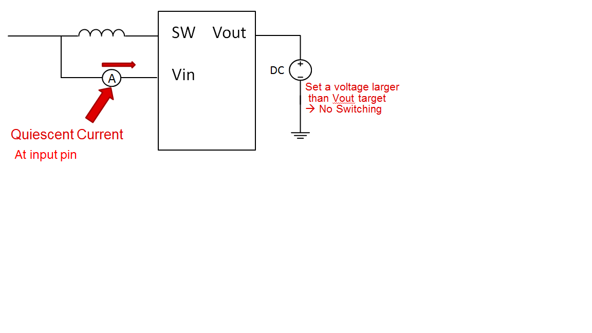
I am struggling to get the quiescent currrent down to 100-200uA uA as suggested in the datasheet. It seems every time I build and solder the board I get a different quiescent current mA draw. 5mA, 8mA, 12mA, 9mA. It keeps changing every time I re-solder the board or check, clean and replace the feedback or comp components. 

I had a similar problem with the evaluation module board. I replaced the feedback resistors to change the output voltage to 12V. I had to clean and re-solder these resistors 5 times before I could achieve 470uA quiescent current as I kept getting several mA current draw. This is still higher than 100uA suggested

So it seems that the component is very sensitive to how the IC and the feedback components are soldered and it is very hard to achieve the low quiescent current reliably. 

Can you offer any advice as to how to make this more reliable? I'm sure in production using reflow soldering things might be more reliable, but I should be able to get it to work in prototype. 

Thanks in advance

David

  • David,

    When the mode pin is connected to the GND, and let the converter works in the PWM mode, the no load current will be big, in mA level.

    When the mode pin left open, the converter works in PFM mode, the no load current will be small, in uA level.

    In no load condition, the IC is still switching.

    But the quiescent current in datasheet is tested when the IC is no switching.

    So no load current and quiescent current is a different item.

    What is your application, could you let the mode open and make it work under te PFM mode? thus the no load current will be much smaller!

    BR,

    Helen

  • The following picture gives out the quicesent current test at Vin pin. So it is different with no load current you tested.

  • Hi Helen

    Thank you for the reply. 

    Yes, I have left the mode pin floating. I understand how the FPFM mode works. 

    So what quiescent current can I expect under no load? As I said, it seems to vary dramatically. Using the EVM I have achieved 470uA which is good enough for me. >1mA is too much. 

    Do you have any advice for setting my comp and FB resistors to minimise the total no-load current? 

    Can you think of any reason why it is varying every time I solder the board? It seems very sensitive. 

    The one comment I can make is that the EVM board with low Iq shows less switching on the SW pin compared to the other boards with higher Iq. 

    Thanks

    David

  • Could you please send the waveform relaing to different no load current to me? generally, with same parameter, the no load should be nearly the same.

  • You mentioned that no load current for each solding is different? did you change the IC ? or just the resistors around the IC? Could you please tell me the input voltage and output voltage?