This thread has been locked.

If you have a related question, please click the "Ask a related question" button in the top right corner. The newly created question will be automatically linked to this question.

TPS6123x burn

Other Parts Discussed in Thread: TPS61230

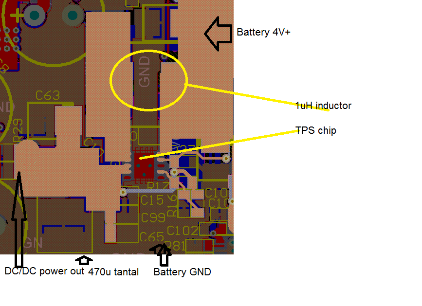
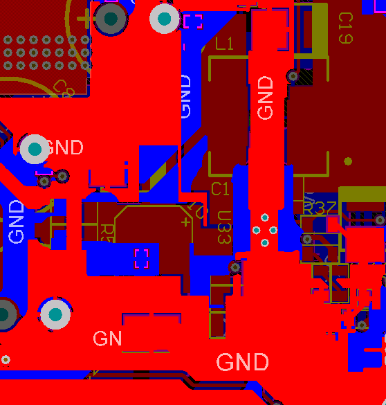
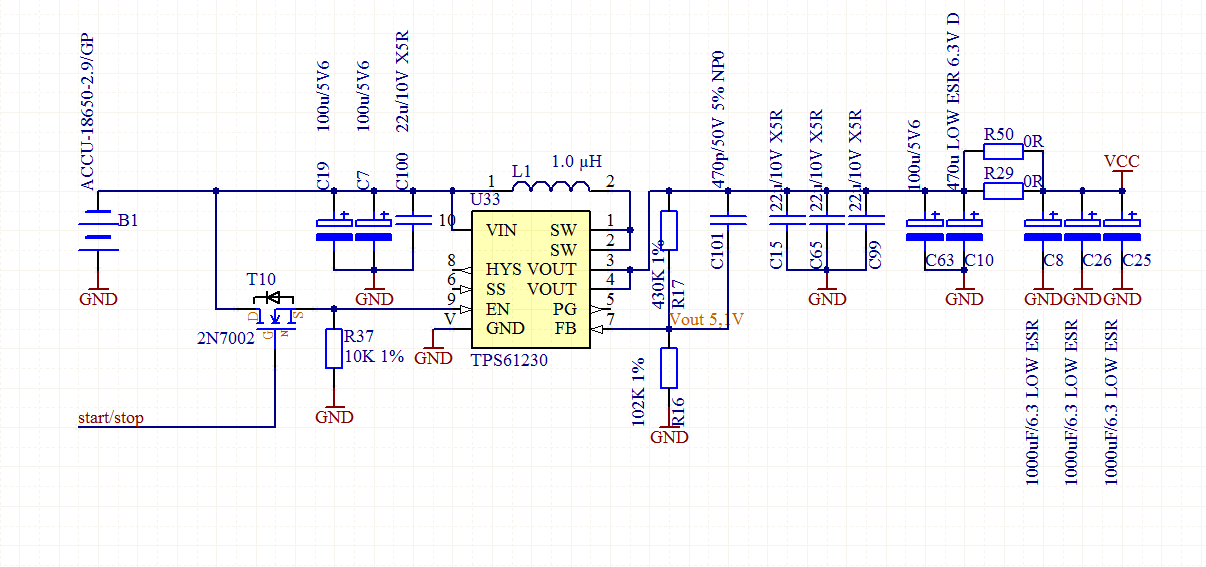
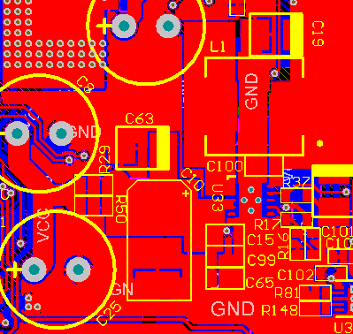
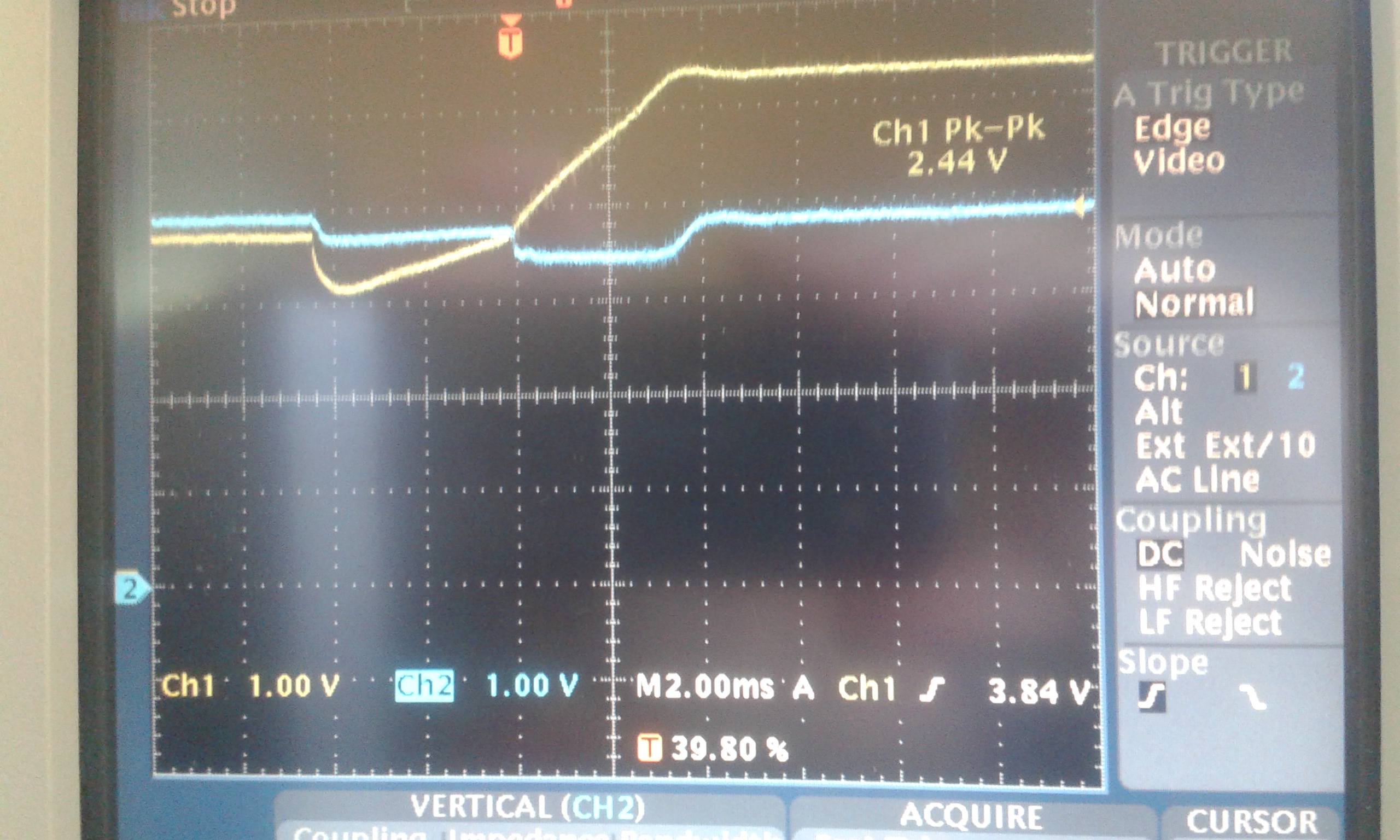
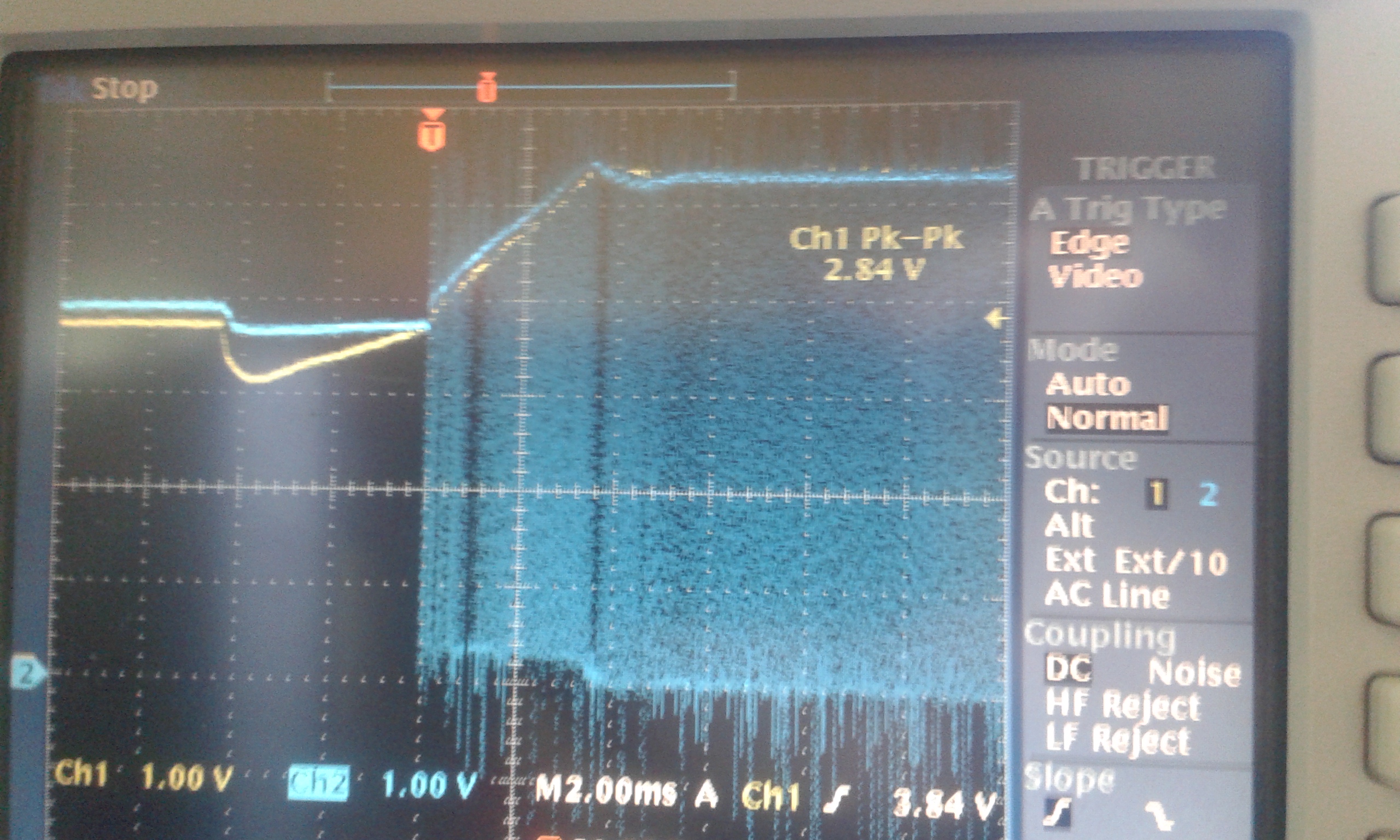
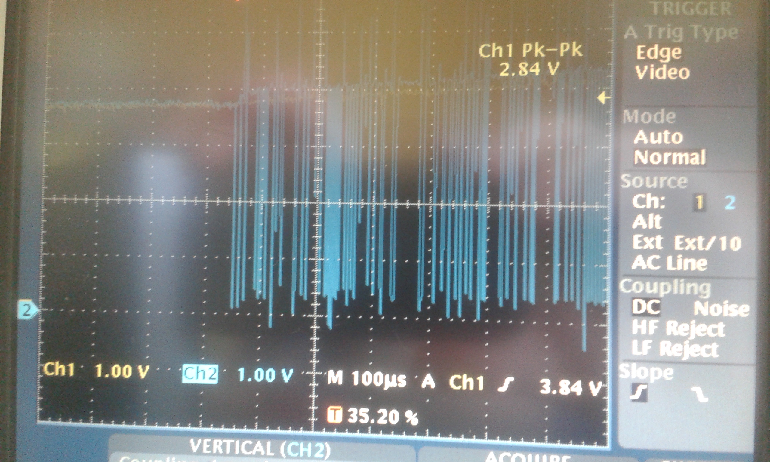
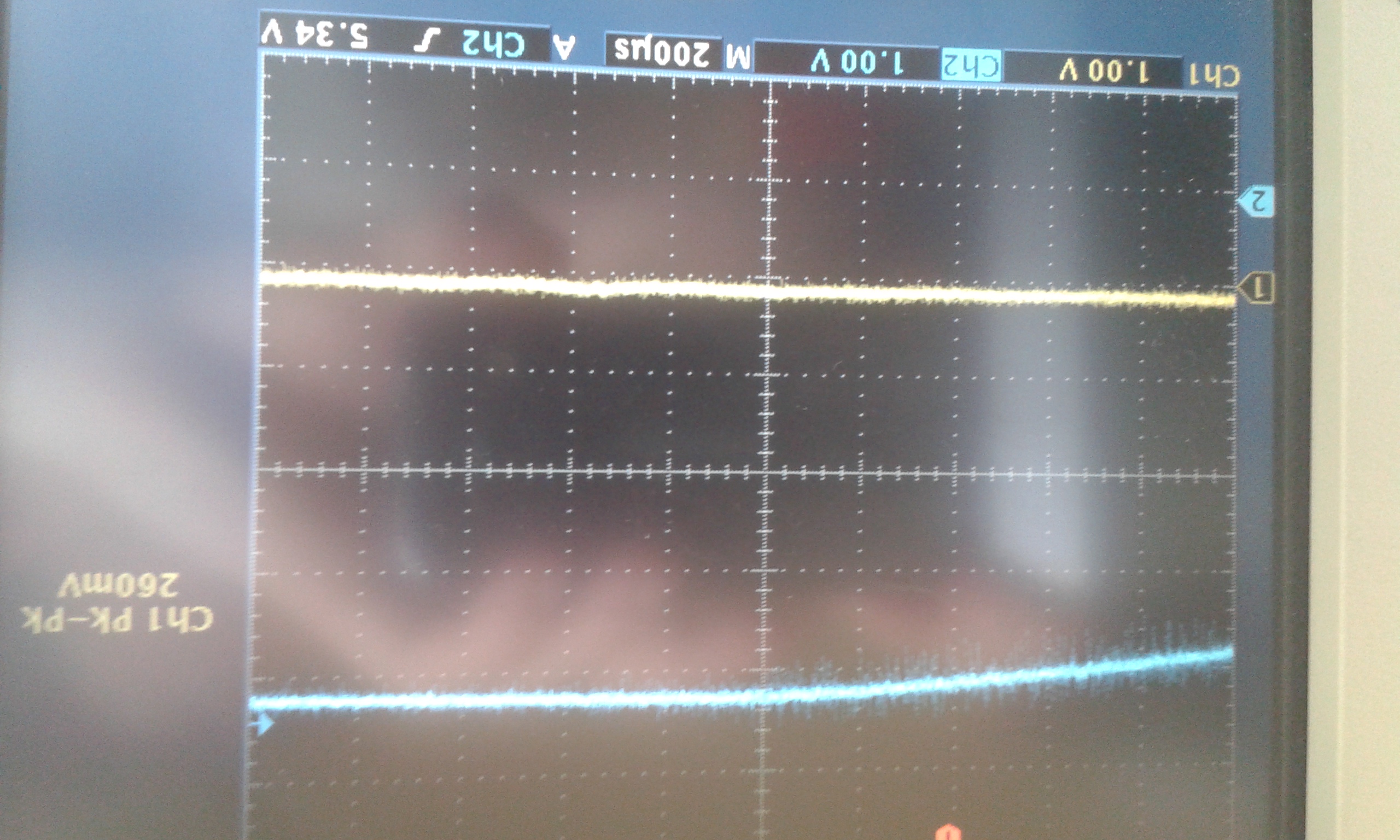
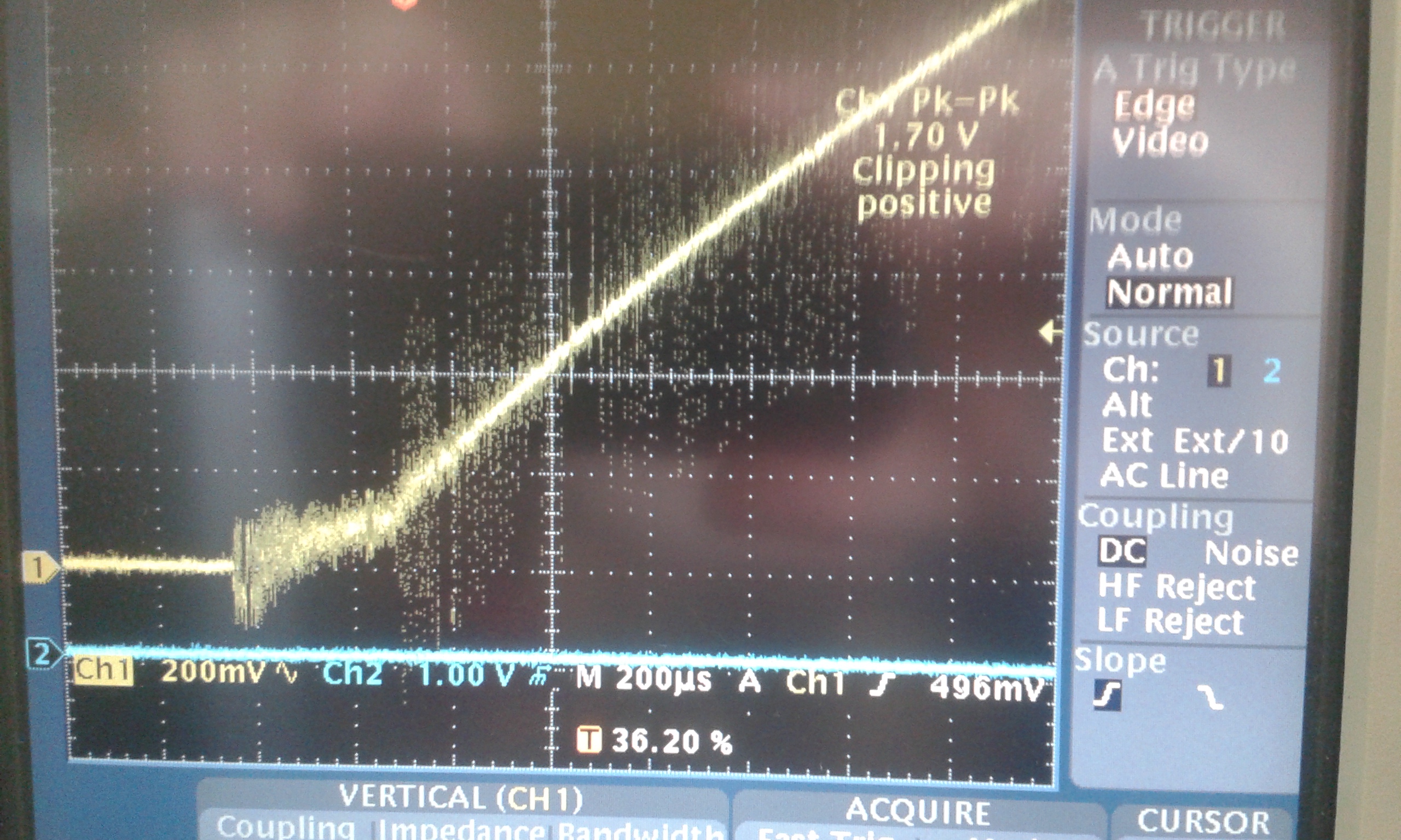
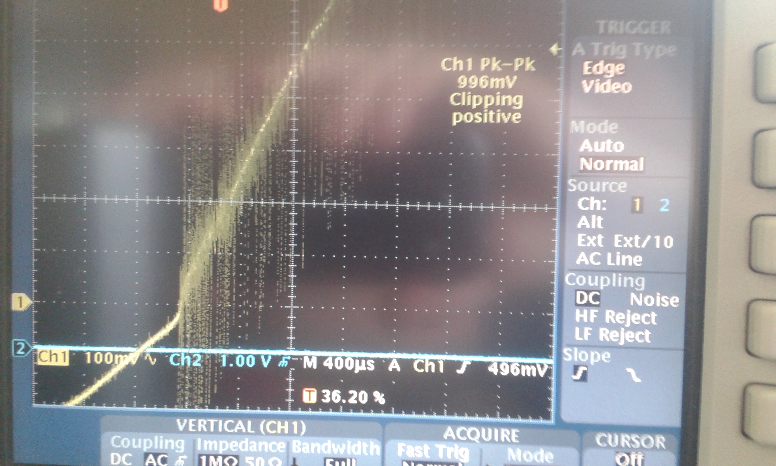
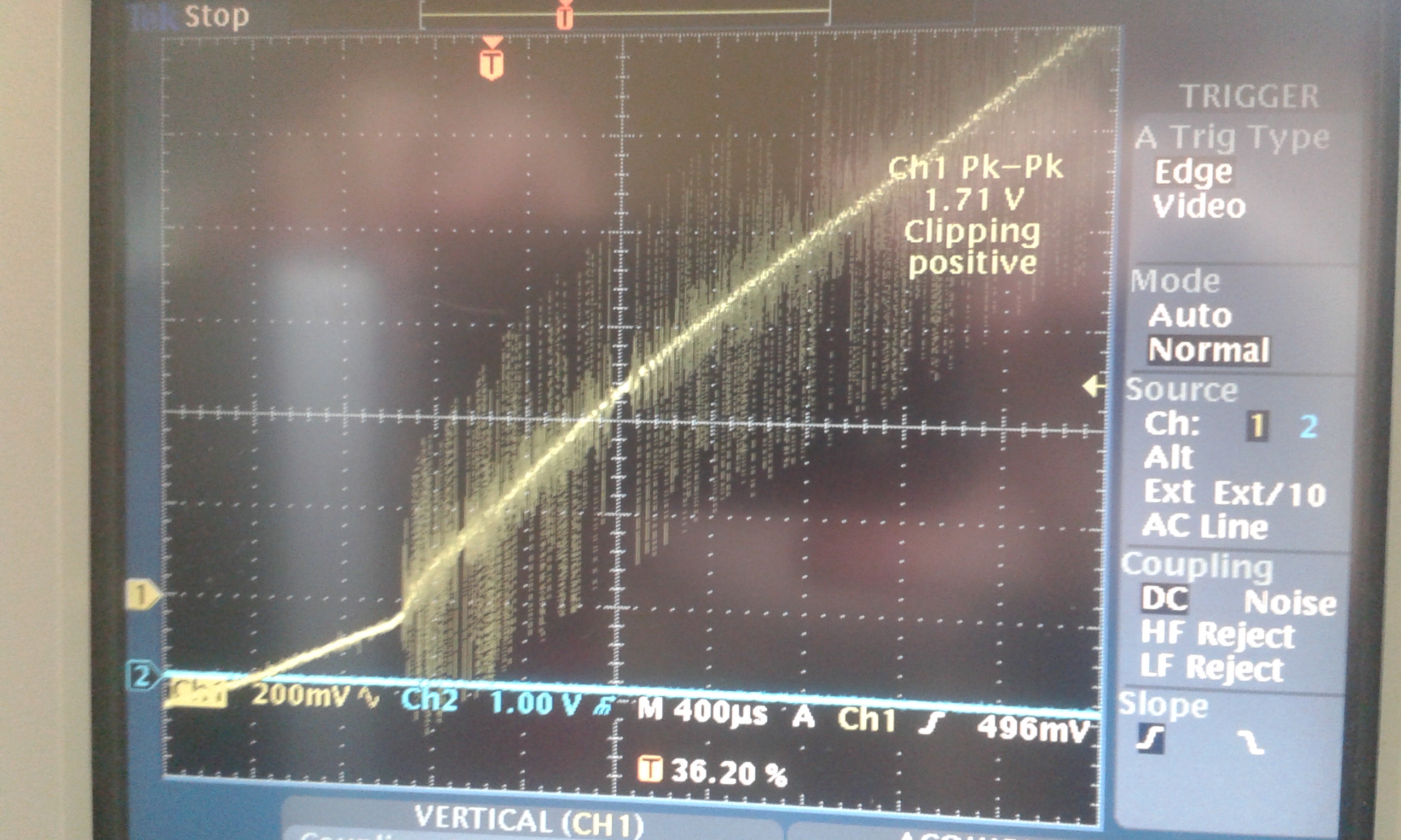
Hello. I use TPS6123x as typical DC/DC step up converter form Li-ion cell (3-3-4,2V) to 5.15V DC 1,5A power out.

My problem is that TPS is occasionally  damage  (burn). Unfortunately it caused burn whole PCB....... (high energy from Li-ion cell)   

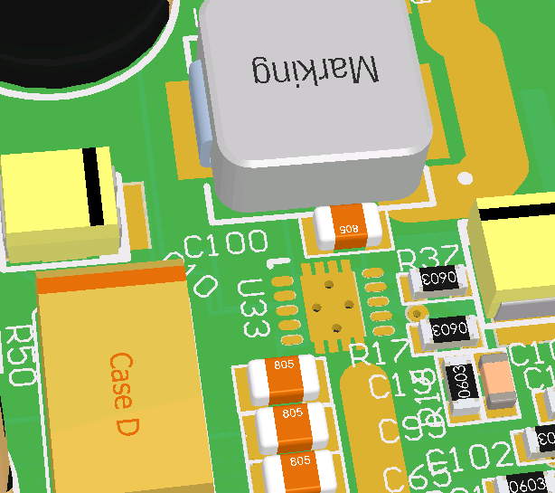
It is typical application exactly within TI suggestion

I have two exception:

1) no capacitor connected to SS pin (soft-start)

2) other inductor, as suggested (manufacturer wurth  74437346010 parametrs:

L=1uH

IR= 8A

Istat=22A

Ddc=8,3mOHM

Fmax=54MHz

My question:

is possible that other inductor (very similar) ro no SS capacitor will caused burn DC/DC converter?

Thanks for any answer.

  • I don't think the SS pin or the inductor is the root cause. please share your schematic and layout image. and at which condition, the device burn.
  •    Hi Jasper, thanks for answer.

    The burn conditions are unknown, but my investigation and research can reproduced burn, but it depend on chip.....

    in my device returned from terrain (burned TPS)  i was replace this chip an continue research,

    so replaced chip was burned in following condition:

    The converter was launched, but no lead , after few minutes i made short circuit VCC to GND (less than 200ms) , the chip immediately burn.

    so i was replace one again damaged chip, and continue test short circuit with poly-switch (2,6A) and next with out poly switch, and no effect, all are OK, I can't reproduce burn out...... in none case.

    It look like that , it depend on sort of chip tolerance.....

    please look in schematic (partly simplified for better understanding)   and PCB layout (.png) and Atium PCB

  • the COUT and the IC are connected on the same layer, right? if yes, the layout look OK.
    could you help to check the stability of the boost converter? and optimized the Cff, Refer to this application note SLVA289
    it seem the device is only damaged by short circuit from your experience, correct?
  • Hi Jasper

     COUT, are you thinking about 3x capacitor 22u/10V X5R (marked on my schematic as c15,c65,c99)?

    if yes, capacitors are connected on the same layer, please take a look that i have additionally tantalum capacitors connected on in input (2x 100u)  and output 100u +470u, also very close on chip and connected on the same layer.

    from my experience:
    series 20 pcs devices as prototypes was launched with positive results (all was tested on maximum lead DCDC converter >1,5A /5.15V ) . it works exactly  as expected.

    at the moment i have 4 cases burnout DC/DC converter

    My research take unstable results:

    in laboratory i have 1 case, where short circuit  damage TPS immediately , and one when NOT (even if it is permanently long time short  circuit VCC to GND )

    please notice that DC/DC converter is started only on demand where main VCC (external for other sources ) was dropped  bellow setting, and measured by MCU (in this case <4.9V)

    So, maybe important is that TPS have 5VDC on back side, form external sources?

    in some cases to major functionality is increase (stabilise -fill)  main VCC  5VDC (from external supplier) when this dropped bellow mentioned value......

    I research also case when DC/Dc are launched without lead, i tried  (multiply time) connect to output , large area of capacitors  20X1000u (discharged) , for simulate current hit. but this no causes damage DC converter,  in none cases.

    Now, i am afraid start  production with more quantity series.......


  • this device doesn't guarantee short circuit protection. the device could damage in some short circuit scenario.

    in your application, if there is not short circuit condition, the damage may cause by other reason. normally, the damage could cause by high current or high voltage, so
    1. could you please to measure inductor current in all the condition, especially in the transient condition, to check if there is a scenario that the inductor is out of control.
    2. could you measure the voltage spike between SW pin and the GND pin with probe (set the probe full bandwidth) to check if the damage is caused by the voltage spike? make sure the measurement loop is small to avoid noise coupling.

  • Hi,
    This device (within block diagram) have build in current sense control (for what ?)
    point 1 and 2. when the inductor is out of control, and how avoid if it occur? , change inductor with increased (eg >10 mOhm) DC resistance ?
    I think that in rely, is less probably that short circuit occur......

    in lab this was reproduced as one for other possibility....
    I think that in relay, it occur randomly, due to start DC/DC converter

    In destiny application DC/DC working maximum 10 minutes/2hour cycle (if main VCC dropped occur) and lead DC/DC is average less than 1A.
  • if you mean the high side MOSFET current sense, it is for the control topology, "constant on time, valley current control. " it is also used to limit the output current at boost mode (VOUT>VIN)

    if the inductor current get out of control, and reach several tens Amp, the device could damage. I asked this question, because i try to find the the condition that the tps61230 becomes damage. then i'll try to reproduce it in the EVM and find the root cause and solution.

    could you help to test the waveform SW, VIN, VOUT and inductor current at the time the TPS61230 is enable by the MCU? you can test the waveform in the good system board. i want to check if the device operates normally in the system board after the device enable.
  • Hello Jasper/I will prepare mentioned waveform soon.

    You prefer with lead, or without?

  • Not sure what is your meaning of "with Lead or without".
  • hello Jasper i t thought  about conditions for  waveform:

    please take me rules for measuring, my DC/DC converter should be  be work  in range  0-1,5A/5,15V.

    I need to know current output for waveform..... and input voltage.....

    regards Mariusz

  • the test condition should be VIN=3.6V, IOUT=1.5V. please measure the waveform at the moment that the boost is ENABLE and startup to switching.
    and also the waveform after the device is stable and operates at VIN=3.6V, IOUT=1.5V, VOUT=5.15V condition.
  • Hello Jasper.

    I the probe was done. In case voltage between GND and SW pin

    You can see two case 

    1) voltage drop (current on track between accu and chip) (unknown resistance but probably  ~~40mohm)

    2) SW-GND normal work with full lead

    3) SW-GND in start converter

    4) Out - GND  voltage output on start

    Do you have an idea how to measure current inductor without increase inductor circuit resistance ?

    current coil is difficult to measure so i made measured voltage droop on track from accu to chip. 

  • 1. the inductor current should be measured using current probe. place a wire in series with the inductor, and measure the current flowing through the wire
    2. for the fourth waveform, the VOUT drop down 3.2V then ramp up. may i know why? could you measure the VIN and SW at this period?
    and i don't see problem in the other three waveform
    3. there is an external power supply connected to VOUT of the TPS61230 as mentioned. does the power supply sink current? i just want to confirm that the external power supply does not sink large current and damages the TPS61230.
  • Hi Jsaper.

    in this example DC/DC converter will start only from accu. (no external supply on back side). Load are other electronic devices with large capacitors.......   

    Unfortunate I don't have current probe,

    even if I will have then this measure can be  very difficult  (this need de-solder coil)


    what i can do at this moment...  buy very small resistance resistor (1mOhm), and measure via scope voltage droop. but this will change coil circuits.


    1) VIN (blue)  vs Vout (yellow)

        Vout  vs SW

    the same but.

  • yes. it is hard to measure the inductor current with current probe.
    from the VIN , VOUT, SW waveform, the device operates normally. so don't need to measure the inductor current.
    could you measure the load transient performance according the page 5 of application note "SLVA289"? i want to check the stability.
  • Hi Jasper.
    please look in my measure circuit. I think that it is OK.please confirm.

    What signal i can use for trigger probe?  in mentioned document is used load current  (in my circuit I don't have this possibility)

    what should be expected  time-line in oscilloscope ?

    In this case i used slope for trigger

    within mentioned document my R1=430K R2=102K C=470p

  • in this post You can see simplified block diagram my module with DC/DC converter  for better understanding whole work condition:

    My module is marked in breaking line:

    CPU control  5V line from external AC adapter, when 5V is dropped or no 5V from Ac adapter, then CPU do:

    left switch turn OFF

    TPS switch ON

    right switch turn ON

    CPU is supplied directly from accu.

    normally when main 5V is ok (99,999% time of work) , left and right switch are in ON state.....

    so, in normal state, TPS have 5V  from main 5V whole time..... (back side)

    Is possible install module in HOTPLUG mode when

    main 5V is present from AC adapter, but TPS is working mode, because module is before plug-in to circuit and not "see" yet main 5V from AC adapter.

    In this case, is possible that in short time (5ms) that AC adapter (by schottky diode)  and TPS supplied right load, together with AC adapter  ,

    After plug in module to circuit  (hot-plug)   then CPU measure 5V from ac adapter , and switch OFF TPS converter, turn "ON" botch switcher, in this mode right load will supplied directly from AC adaptor.       

  • 1. the measure setup is good. you can just measure the VOUT ripple when the load is switching between 0A and 1.5A. the VOUT ripple should be level of 100mV~200mV. the time scale 100uS to 1ms

    2. during the 5ms, the AC adapter connect with the TPS61230 output through the schottky diode. i don't see risk of damaging the TPS61230, unless there is a high voltage at the output pin of the TPS61230

    3. when the AC adapter is on, the two switches are both on. when the adapter is gone, you just need to turn off the left switch, then turn on the TPS61230. why need to turn on the right switching again? not sure if there is bulk capacitor connected to the right side of the right switch.
    if yes, large inrush current would flowing through the TPS61230 when turn on the right switching and damage the device.
  • Hi Jasper.

    point 2) AC adapter powered 5V - 5.2V and module with TPS delivery 5.1-5.2 V depending on load (this are  very similar  voltage)


    point 3)

    The idea is: powered right load in all condition (if AC adapter are dropped or gone) by AC adapter or by TPS6123.

    we have three case:

    first), normal working, module is plugged in circuit,  AC adaptor is OK and measured 5V by CPU is OK, then both switch are in state "ON", TPS in "OFF" state , left load is powered by AC adopter directly , right load is powered from AC adapter trough  by both switches.

    second), normal working, module is plugged in circuit, AC adapter is fail (measured 5V by CPU in module reports that is less than 5V or 0). then module go to state: left switch go to "OFF", right switch continue state "ON" and TPS go to ON,  in this case right load have always 5V whole time.

    there) install mode in this case module isn't on the circuit, but is running. 

    left load are powered from AC adapter, right load isn't not powered because module is plugged OFF

    in this mode TPS is in "On" state right switch is in "ON" state, but TPS are working without load. (no connection with right load)

    next the working module is plugged-in circuit  in this time right load will powered together  for AC adaptor by diode in module, and from TPS by right switch. 

    when module is plugged in circuit CPU measure 5V form AC adapter and module continue normal working.


    in question large capacitors You have right  is possible current hit, because in load right i have 4000uF

    but in my module i have also 4000uF connected directly to output TPS for storage energy  when 5V dropped, and balance current hit.

    It is second generation module, I think  that idea is corrected  (used the same solution switch, diode, etc)

    in first generation was used MAX1708,

    in population more than 5000 pcs and 5 year experience working isn't unknown case damage DC/DC converter

    I decided use TI solution, because maxim is expensive and take more space PCB.


    What i can do something else ? 

    i need resolve problem... Are You sure that magnetic parameters are OK?


    I hope that this description should clarify idea and all condition for TPS.

    Best regards Mariusz


  • when the TPS61230 is on, and the right switcher change from off to on . there is risk that the TPS61230 could damage if the right load voltage is very low, because the VOUT may drop down to a voltage lower than VIN. . this is some think like short circuit.

    would this scenario happen in the real application? this is only the risk that i can see to damage the device. VOUT drop down to lower than VIN during the TPS61230 is operating.

    if happen, could you avoid this? turn on the right switcher before turn on the TPS61230.

    Magnetic parameters you mean the inductor? i don't see problem of the inductor
  • Hi Jasper.

    OK.  I understand,

    when is install mode always right load is 0V......

    if the chip isn't immunity to short-circuit, then i don't see solution.

    some chip based on non representative parameters work correctly, and some will damage.

    The main problem is that module doesn't know when is mode install. and always exist risk current hit from right load.......


    Is no possible "delay start" because module doesn't recognise when is install mode or when is 5V dropped, from point off view module, the are the same condition.

    This know only customer who will install module.


    Do you know maybe about other TI solution, protected by short-circuit (best 1:1 replace).

    or how to protect TPS in this case:

    polyswith for right load? (i have place on PCB to install this, now 0R is mount)

    What do you think about increase capacitors on output TPS from 4000uF to 6000uF?

    other solution?


    In second hand, I tested short-circuit  by connect discharged to 0V large capacitors  area (more than 20000uf as right load) when TPS was in on mode.....

    but I know, that in some cases (none representative) this test can pass..... or not

    please look on updated block diagram (it is fill on real capacitors value, on side module and right load)

    What can be maximum capacitor on output TPS? it is limited ?


  • We don't other device can meet this requirement. could you turn off right-switch and have a resistor (10ohm for example) in parallel with the right-switch. when there is not load (the module not plug in), the right side voltage is 5V. when the module plug in, the voltage will drop down.
    then the MCU know the module plug in. then turn off the TPS, turn on the right_switch, and turn on the TPS again.

    increase the capacitor to 6000uF should not help, considering the VBAT could be 4.3V, very closed to 5V output.
  • Hi Jasper.

    within your opinion, You claim that damage TPS can only occur when module is installed  in circuit (TPS is working),

    so the load capacitance do short-circuit it can caused burnout the TPS. Yes ?

    the solution will be

    detect that module is installed or not, and if no installed the TPS could be in off state. Yes?


    other question.

    Is possible that module installed on circuit, and AC-adapter is switch off state. In left, and right load are 0V

    Can i turn ON TPS (where) left switch is in state OFF, right switch is in state ON,  right load is 0V, total load capacitance is 10000uF?  is it safe for TPS ?


    regards Mariusz

  • it is the highest risk to damage the device from application condition.

    yes, short circuit could damage the device.

    yes, and other solution maybe you don't need to turn off the TPS, just limit its output current, make the VOUT is not drop down below VIN.

    i experiment with EVM, startup the device with 10000uF for 0V. i observe the inductor current. the current is under controlled. so it is safe.

    by the way, please make sure the device is stable.
  • Hi Jasper.

    I have idea how to recognize that module on circuit or not, So it should be resolve problem Hot-plug module, and exclude short-circuits event.

    abuot:  "please make sure the device is stable."

    My scope  waveform was as attached pictures . I don't see typical Waveform pattern within SLVA document (by DC/Dc started)

    What  do you need else, to confirm that the device are stable or not ?

    blue line = measured voltage output when DC/DC are starting (full load 1,5A capacitance  4000uF from 0V )

  • could you measure the VOUT transient waveform (IOUT = 0A->1.5A)? the VOUT waveform should be AC coupling. and scale should 100mV/div.
    you can capture the waveform when a load, such as 3ohm resistor, is connected to the output of the boost converter. you'll observe the VOUT drop down several 100mV, then increase to normal voltage.
  • Hi Jasper.

    I need make sure.

    1) You need as load pure resistance load 3 ohm without output large capacitance ?  only  3x  22uF like in reference ?

    if yes follow is waveform in mentioned condition (pure 3 ohm resistance only 3x22uF on output TPS).

    it is right measure as You expect  ? (within SLVA condition)

  • no. i want to know the stable in your final board, 10000uF, not only 3*22uF.
    i'll check with my EVM later, and share you the waveform.
  • Hi Jasper

    I made few pictures with different  base time

    so first three, presents when module isn't on circuits.(without right side load)
    in ths case on TPS output is connected 3x1000uF (aluminium)  and 470uF (tantalum) and 100uF (tantalum),  in this case, load for other PCB elements is very low..... <100mA

    next pictures presents waveform when module is on circuits (right load side is connected for TPS)

  • Attachment is my measurement with the TPS61230EVM and 10000uF output capacitor. it seem good.

    what you attachment should be startup waveform, i don't see problem from the waveform

  • Hi Jasper.

    thanks for answers, What i can improve else to avoid burn:

    Do You think  that  exclude short-circuit (large capacitance- connected  when TPS is running) should be resolved problem?

    Regards Mariusz.

  • yes. short circuit is only the risk i can see to damage the device. do you have a way to validation your solution (exclude the short circuit).
    do you repeat the damage again or it is the former one?
  • Hi Jasper,
    according to my last picture (show burnout TPS), it is third case damage TPS, (old)
    From my experience:
    I have one PCB with TPS, where I can't damage in any way.... (also hard short -circuit), first TPS in the same PCB was burn, when short-circuit was done, immediately....., after replace for other chip, this chip is immunity for all.
    It look like depend on chip tolerance......
    I will introduce software solution, that TPS will switch off, when module isn't plugged, to avoid capacitance short current hit.
    I hope that it will help.....

    Thanks for assistance.
    I will let know about results before introduce software solution, but it can take time for tests......
    BR Mariusz