This thread has been locked.

If you have a related question, please click the "Ask a related question" button in the top right corner. The newly created question will be automatically linked to this question.

TPS62133 Fails Sporadically

Other Parts Discussed in Thread: TPS62133, TPS62135

Introduction

Dear TI Team

We are currently struggling with a new PCBA where we use a TPS62133 to convert 12VDC to 5VDC. On a first validation batch of 60 boards, about 15% of these boards the TPS62133 (U301) failed after 1-10 days of operation.

To start the discussion I’ll try to provide a more detailed description of the problem below.

As we run out of ideas where the problem could come from or how to solve it, we would highly appreciate any input or ideas.

Best regards

Diego


Failure Description

-          Out of 60 boards 8 boards (ICs) failed

-          The failure happened

  • on 6 instances in the first 1-4 days of operation, on the other 2 instances after about 10 days of operation.
  • When the system was in “standby” – in this state the converter is loaded with about 1A by an “embedded linux module with an LCD display”

-          The failure was

  • On 7 of the 8 failed boards, the 5V output was not there anymore. On 1 instance the 5V was output was gone and additionally the 12V input was shortened.
  • Replacing the TPS62133 solved the problem on all of the failed boards

-          Additional comments

  • On the board there are 2 instances of the TPS62133-based DC/DC converters: U300 and U301 (see schematic). U300 never failed so far, but it is also loaded a little less (about 0.5 A) and the layout is minimally different.


Current schematic and layout

-          Note: U301 failed sporadically (U300 is just shown for sake of completeness, e.g. with respect to thermal considerations or similar)   


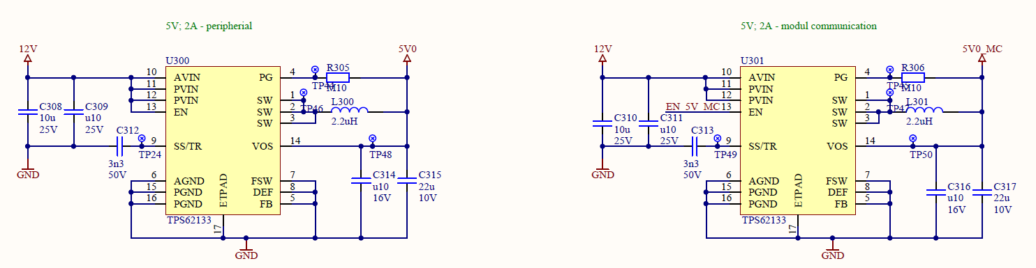
Top layer and top overlay                                          

Bottom layer and top overlay


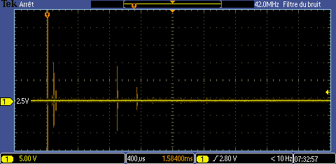
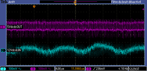
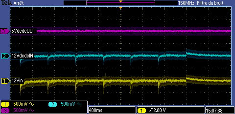
Measurements of input-/output-voltages

-          Switching 12V input “on”:

-       5VdcdcOUT corresponds to 5V0_MC

-       5V0_MC is loaded with about 1A by a LCD/backlight module.


-          System in “standby”:

-       5VdcdcOUT corresponds to 5V0_MC

-       5V0_MC is loaded with about 1A by a LCD/backlight module.                                  


-          System during “normal usage cycle” ”:

-       5VdcdcOUT corresponds to 5V0_MC

-       5V0_MC is loaded with about 1A by a LCD/backlight module.

-       Note: The “spikes” on the 12V input are due to load transients (~2A) on the second TPS62133 regulator generating the “5V0”.

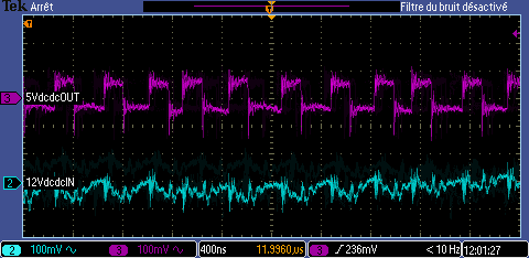
-        System in “standby” – measured on a modified pcba:

-       For this measurement a second 22uF capacitor was soldered on parallel to C317.

-       5VdcdcOUT corresponds to 5V0_MC

-       5V0_MC is loaded with about 1A by a LCD/backlight module.                                  


Temperature Measurements

-          Measurement setup:

  • The measurements were done using thermocouple (elements/sensors) and a UT71E multimeter.
  • The thermocouple was placed either “on the top of the case of U301” or “on the bottom side of the pcb at the center of the thermal pad of U301” in both cases using “thermal heatsink paste” to get an acceptable thermal contact.
  • The system was left powered for a few minutes till the temperature was stable.
  • For these measurements the output 5V0_MC was loaded (by resistors) with 1A, 1.5A and 2A.

-          Measured temperatures (after about 5 minutes of operation):

  • At 1A (resistive) load
    • Top of case of U301: 44°C
    • Bottom side (vis-à-vis thermal pad): 43°C
    • Estimated/calculated chip temperature : 52°C
  • At 1.5A (resistive) load
    • Top of case of U301: 59°C
    • Bottom side (vis-à-vis thermal pad): 53°C
    • Estimated/calculated chip temperature : 70°C
  • At 2A (resistive) load
    • Top of case of U301: 80°C
    • Bottom side (vis-à-vis thermal pad): 70°C
    • Estimated/calculated chip temperature : 95°C
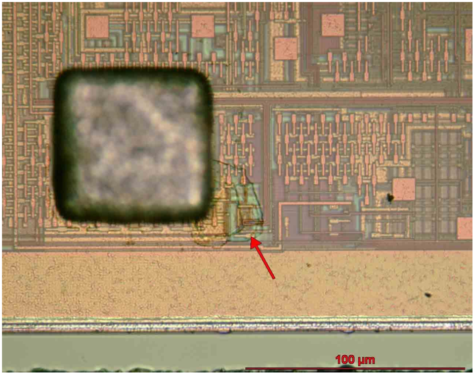
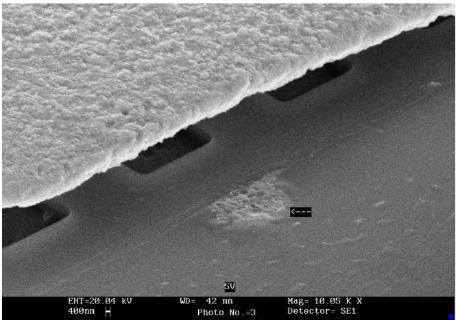
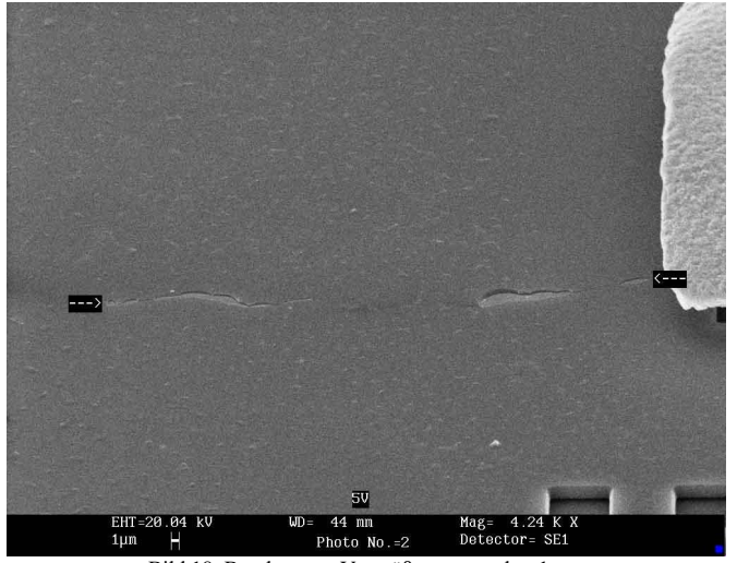
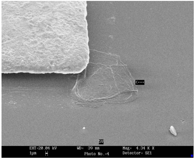
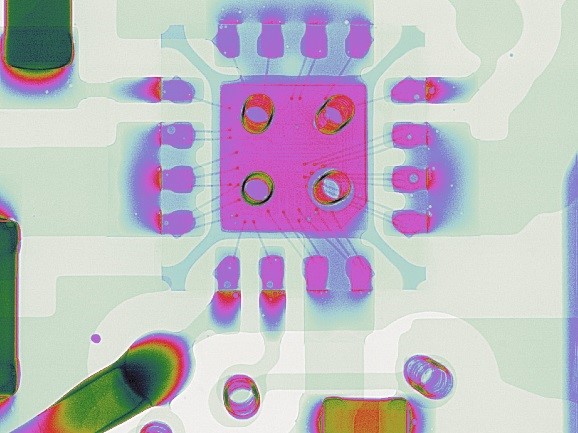
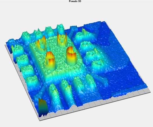
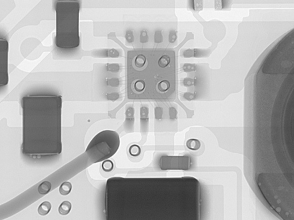
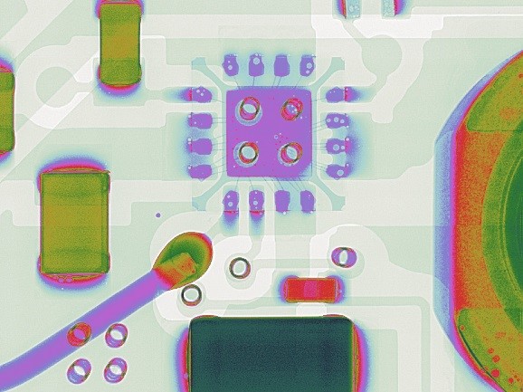
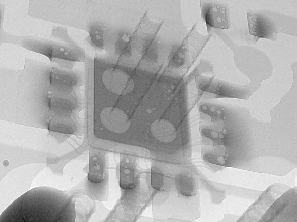
 

X-Ray analysis

-          Initial comments

  • So far only 1 boards/U301 were x-rayed.
  • 1 of these boards had “failed” before x-raying
  • 1 of these boards had worked for several weeks (without failure) before x-raying.
  • It seems that there was no significant difference and the wetting/soldering of the thermal pad seems ok.
  • X-rays of approximately 30 more boards will be added soon.


-          X-rays of a “failed” board


-          X-rays of a “good/working” board


Theories and Thoughts

-          Over-/Undervoltage problem

  • Seems to not be the cause because
    • no voltage measurement showed spikes/peaks exceeding maximum values.
  • Anyway it may be a problem because
    • A “failure” could never be observed “directly”. The measurements were done on a “working” board, which may show a different behavior than a board that would fail after a few days.

-          Thermal problem / Overload

  • Seems to not be the cause because
    • The thermal measurements showed, that the temperature should be acceptable at the given load (1A) and even at higher loads (1.5A)
    • No failure could be “produced/reproduced” when intentionally “heavily using the system” (which results in maximum realistic load)
    • No failure could be produced when powering the board at 70°C environment temperature, even at higher loads (1.5A) then in the system.
    • No failure could be produced, when shorting the 5V0_MC during 5 minutes (which results in a 4A load current)
  • Anyway it may be a problem because
    • Only 4 vias are used.
    • These 4 vias are “plugged” and seem “hollow” (see x rays)

-          Batch/IC series problem

  • Seems to not be the cause, because
    • the second DCDC-converter (U300) never failed
  • Anyway it may be a problem because
    • U300 is loaded differently (and also the layout/location is slightly different)

-          Production problem / bad thermal contact on some boards

  • Seems to not be the cause, because
    • The first 2 x-rays showed no significant difference and looked “good”
  • Anyway it may be a problem because
    • Only 2 boards were x-rayed so far

-          Capacitor related problem (see voltage measurements above)

  • Seems to not be the cause, because
    • The capacitor(s) should be ok for the given load according the recommendations in the datasheet.
  • Anyway it may be a problem because
    • The “pulses” on the 5V0_MC output (~100mV) seem a bit too big and are drastically reduced by placing an additional 22uF capacitor
      • Note: as 22uF ouput capacitor (C317) “Murata GRM31CR61A226KE19L” are used.
      • The datasheet of TPS62133 (SLVSAG7C –NOVEMBER 2011–REVISED JANUARY 2015) indicates in Figure 26, that the “output ripple” should be below 20mV.
        • It is though not totally clear what “output ripple” means in this context as e.g. Figure 32 indicates that the “noise” on the Vout is about 100mV (peak to peak).


Other information

-          A new production batch of the same board is currently in production.

  • This new batch is subjected to a “burn-in” test
    • In this “burn-in” the boards are powered in an oven at 70°C environment temperature, while loaded with 1.5Ampere (resistive load), during 5x24h.
    • So far 2 boards out of 30 showed the same defect (U301 fails) during this “burn-in”
  • Thanks for such a detailed post.

    Could you share the part numbers for your inductor and the rest of your caps?

    As well, what is going on with your system when the system is running for days?

    How did you determine that no spikes were present on Vin?

    Since you seem to have somehow repeatable failures, it is most useful to capture the moment of failure the scope to see what is happening. Can you probe Vin, Vout, SW, and load current and trigger on Vout falling?

    Do you have a local TI FAE?
  • Thank you for the quick reply.  My "answers" are below.

    Best regards, Diego.


    Current BOM (relevant parts only)

    - U301: Texas Instruments TPS62133RGTR

    - C310: Murata GRM219R61E106KA12

    - C311: Murata C0603C104K3RACTU

    - C313: Murata GRM188R71H332KA01D

    - R306: Vishay CRCW0402100KFKED

    - L301: Bourns SRN8040-2R2Y

    - C316: Murata GRM155R71C104KA88D

    - C317: Murata GRM31CR61A226KE19L

    What happens when the system is "runnig for days"?

    Practically speaking the system can be in 2 "major" states: "Standby" or "In use"

    - In "Standby":

    - Essentially a display module is running and consuming current from 5V0_MC (about 1A). The display "cycles" some videos and therefore (and also because it is an embedded Linux board) can cause small load changes depending on the CPU load and displayed image.

    - "In use":

    - During a normal "use cycle" (about 30s), the display keeps running as before, but additionally some motors/valves/power-leds are switched on/off a few times.

    - The (main) load for the 5V0_MC is still the display module

    - One of the motors and one power-led that is swiched on/off, is powered by the second dcdc converter / 5V0. This generates a load change from about 0.5A to about 2A on this 5V0-converter but should not affect the 5V0_MC

    - All other motors/valves/power-leds are powered by the 12V input voltage (using FET transistors "driven" by the 5V0_MC or 5V0). They therefore do not cause (significant) load changes on the 5V0_MC as well. But that is the reason for the "peaks" on the 12V signals in the scope images above.

    When the system is "running for days", the system is 99% of the time "in standby" and the rest of the time "in use". More precisely we typically trigger about 5 "use cycles" (about 30s each) during the day and leave the system "in standby" for the rest of the time (the system is never switched off during "several days").

    How did we determine that no spikes were present on Vin? 

    - We bulilt up the system "as normal"

    - We soldered on a few wires (about 3cm) to both pads of C310.

    - We then connected an oscilloscope probes to these wires

    - Then we typically first "looked" at the oscilloscope during various situations e.g. During standby, turn 12V on/off or in use when some motors etc turn on/off.

    - Then we set the trigger to a reasonable voltage (typically slightly above 12V) and "recorded" the Vin in the situation to analyze ("single run" style).

    - The above was repeated at various oscilloscope settings (time / voltage resolution, ac/dc coupling, filter on/off etc..)

    - Generally we repeated the "switching on/off" also 10 times or more, to have at least a chance to "see" spikes that maybe only come once in a while.


    Doing this, we never saw a spike exceeding about 17VDC on the 12V input. The "worst" spikes we saw happened when "turning on 12V by plugging in the 220VAc/12Vdc power supply into 220V mains outlet" (see image below)

    Schematic of 12V input path (from connector to "on-board-12V"):

    Spike on 12V /Vin when plugging in Ac/Dc converter (here only about 10V but can go up to about 17V. Note: the level seems to depend a lot on the oscilloscope probe/cable "orientation" -> probably mainly a measurement error/induction effect)

    Can we reproduce the failure and "record" some data? 

    Well no, that is a big part of the problem. So far we could not find a way to force/reproduce the error. Therefore we also could never "record/measure" anything during a failure. We tried to "torture" some boards e.g. by unplugging/replugging components when the system is powered, overloading the dcdc converter, run the system at increased temperature but could not find a way to produce the failure.

    Potentially the reason for this could be, that only e.g. 15% of the boards do have "a problem". If this would be true, it may be necessary to "try to produce the error" on about 10 boards to have "a good chance" to have one "bad board" included, and to find out that "this would be the way to reproduce the failure".

    Generally it is not yet clear if "good/bad boards" exist, or if "all boards are the same" (with respect to the failure).

    I would love to set up 10-20 boards and oscilloscopes, set trigger to "Vout falling" and have them running a few days, hoping that one fails and records the event. But we lack of oscilloscopes and (until today) we also did not have sufficient boards to run such tests.

    Do we have a local TI FAE? 

    I guess FAE stands for Field Applications Engineer.

    No, so far we do not have a contact to a local TI FAE.

  • Thanks again for your detailed reply.

    If I understand correctly, you have a motor and some power LEDs on the output of the failing rail, but do not have these on the 'good' rail? Do these loads plug into JP104?

    It is probably worth to zoom in on the spike you show above. It is likely just noise coupling into the probe, as you thought, but it's difficult to tell at 100 msec/div.

    Besides some possible noise on the output and input, my main concern is on the input cap. There is a small but possibly significant layout difference in the GND connection from the input cap to the PGND pins. This connection is longer due to that EN via which is in the way. This adds extra inductance which creates higher voltage stresses on the device.

    As well, the 10uF input cap has a fairly poor DC bias performance. At 12V, it is down to around 1 uF effective C. This is likely too small for a 3A device. Can you try a bigger input cap or a different one with better DC bias characteristics?
  • Hi again

    - No the motor and power leds are on the output of the NON-failing converter. The failing converter mainly powers an LCD/backlight panel plugged into JP104 (plus a few ICs and standard "few-mA-LEDs").

    - Zoom of the spike on the 12V input: well we only have a "bit" of a zoom (not helping a lot) - we could not reproduce the spike anymore at a higher time-resolution setting unfortunately. As the failure does not occur during swiching on (but during standby several days after switching on): how do you think this spike could be related to the failures? Stress which causes failures at a later time?

    - Regarding the inductance/layout difference: Well but we talk about a few millimeters. Do you really think that could be a (part of) the problem? How would you recommend to layout if the EN signal is used?

    - Regarding the input capacitor: This sounds very interesting. I checked it on the murata homepage and have seen the "capacitance change on dc bias" you mentioned.

    We will try to change this capacitor for another one on a few boards and look if a change is visible on a scope. Do you have by chance a recommended capacitor pn/type?

    Best regards

  • Ah, sorry for mixing up the outputs. Of the few ICs on the failing rail's output, would any of these be switching power supplies or otherwise create a lot of noise on the 5V rail? If so, it's a good practice to add a ferrite bead near the loads to keep all this noise off of the output bus.

    DC bias is critical for switching power supplies. There is a note on page 15 of the D/S about this.

    This looks like a better cap in the same case size: psearch.en.murata.com/.../GRM21BR61E226ME44#.html Having a higher nominal value means there is still more effective C left at you bias voltage.

    I'm not sure if you will be able to measure anything different on the scope with the better cap. This mainly helps reduce the voltage stress seen by the device during every switching cycle.

    It sounds like the Vin spike does not correlate to when you have seen the failures, so it can be ruled out.

    The EN via should be kept closer to the IC so that the GND plane can pour it around it better and make a shorter path.
  • In case others are interested in this topic I will try to summarize the "results" below.

    - Modifications of the capacitors and (minimal) layout modifications did not significantly change the behaviour/failure rate.

    - An external analysis showed, that some "micro-cracks" appeared in the TPS62133 (see below). If they are the cause, part of or a result of the problem remains unknown and  also why they appeared on this IC (but not on the other one on the same board).

    - Long story short: we solved the issue by replacing the TPS62133 with another dc/dc converter. It is from another brand, has a SOIC case and operates at lower frequencies.


    Best regards and thanks to TI for the support.

    And last but not least a better picture of the soldering

  • Somehow the pictures did not work in the last post

    Some pictures of the micro cracks:

    And finally FYI a better picture of the soldering

  • Hi,
    I have a very similar problem in my project with TPS62133: it fail without apparent motives.
    Could you try to post the images with the micro crack?

    Best Regards,

    Fabio
  • Hi Fabio

    I'll try. Anyway I wish you good luck with finding and/or solving your problems.

    Best Regards

    Diego

  • I thank you for publishing the images of the micro crack and compliment for your detailed analysis: very interesting the DIE analysis.

    Did TI company ever admit any problem with this device?
    Does the AUTOMOTIVE version have the same problems?

    At this point, since I don't understand the cause of the failure, I think I will revisit my project by replacing it with another DC/DC.

    Thank you again for your analysis,

    Best Regards,

    Fabio

  • Hi Fabio,

    As evidenced by this thread, the root cause of the previous failures was never reached. I can say that we do not ship these ICs with cracks in them.

    If you can start a new thread and post the relevant details of your specific situation (schematic, layout, waveforms, when it fails, etc.), I can assist in your debugging.

    We have also recently released an improved version of this type of 12Vin step-down converter, the TPS62135/6. These are smaller, higher current, more accurate, and with more features.