This thread has been locked.

If you have a related question, please click the "Ask a related question" button in the top right corner. The newly created question will be automatically linked to this question.

High ripple using TLV61220

Other Parts Discussed in Thread: TLV61220, TPS610981

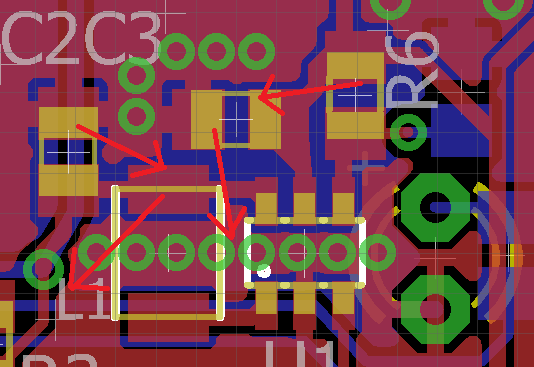
I'm using the TVL61220 boost converter in a battery operated uC/radio circuit (sensor node).

Typically the circuit will be fed using 2 AA cells, but should still operate at a Vbat of around 1v (@Vcc ~3v). The TLV is decoupled with 10uF (X5R MLCC) at the input and outputs, the voltage control divider is 1800 and 360 kOhm.

The circuit is typically at rest, consuming 10's of uA. The other modes are CPU running @ ~3-5 mA and sending a radio datagram the maximum current consumption reaches between 20 and 70 mA. 

When I power the device using 2AA's (~ 3v Vin), the ripple seems acceptable in the order of  10-20 mV. However when I power the device from a single AA, the ripple reaches about 500 mV (!). Adding additional capacity (additional 47uF at the output) lowers the switching frequency considerable as expected, the Vpp ripple is still > 300 mV accouting for a 5-15% ripple on my Vcc.

Are these normal figures for the TLV61220 and if so, which counter measurements can i take to lower the ripple at low input voltages?

Note that we're still in a prototyping phase, so choosing a different, better suited, switcher is certainly a good/viable option. As always we're aiming for highest battery life (south of 3 years).

Picture shows the Vcc ripple with Vin=~1.5v, standard (2x10uF) decouping and the CPU running (consumption ~4mA)

  • The TPS610981 should be better solution for your application, because of the lower quiescent current.

    about the TLV61220, the ripple should be much lower than 300mV for the application condition.
    could you share the schematic, layout and inductor /capacitor part number? these factor could increase the ripple of this devices.
    i would also suggest that you can apply an EVM for reference.
  • Hi Jasper,

    Thanks for the reply. I'd say the 300mv is way too higfh as well :)

    Herewith my board layout, showing the supply part. C2,C3 are the 10uF MLCC's. The schematics are not that interesting. it's just the recommendations as per the datasheet.

    Part no's:

    L1: Murata LQH3NPN4R7MMRE 4.7uH

    C2/3: Yaego CC0805KRX5R5BB106 10uF X5R (also used Tayio Yuden EMK212BJ105KD-T on some boards, didn't measure those.)

    I was planning to stick closer to the reference board layout in the final version of our board. (Note that the "bypass DC-DC" is just an open solder jumper)

  • I guess the C3 is the 10uF output capacitor. the layout is bad. the output capacitor is the most important component, it should be placed closed to IC and connected with short, wide, direct copper. otherwise, the boost converter could operate abnormal or even damage.

    to validate the ripple is caused by the layout. please move the C3 to the top of the IC and connect the capacitor to the IC's VOUT and GND directly with solder. (minimize the inductance between the COUT and the IC)
  • Thanks for the advice, I din't know this C3 was that critical. I will do some measurements tonight with the capacitor directly soldered across the TLV.

    Herewith my improved pcb layout, shortening all critical (return) paths. (note that R7 was moved to the back of the board.) The via most left in the image is the battery feed point.

  • i would suggest avoid using vias. is it possible to layout in this way?

    1. rotate the inductor 90 degree anti-clock

    2. move the C3 close to the left side of the IC and connect to the VOUT and GND without Vias, using wide, short copper

    3. move the C2 a little close to the C3, connect their GND-node directly.

    4. the VIN pin connect to C2 under the C3 (it is possible for a 0603 package capacitor)or through other layer.

    5. the FB node is also important, place both R6 and R7 on the same layer. the FB pin routing should no be too long.

  • Jasper, your help is greatly appreciated! More help than expected!

    Made another layout again, based on your remarks. :) (note the R7 is still on the other side, but total track length is really short)

  • the layout is good.
    after I re-read you first post, another concern is the output capability of the TLV61220 may can't support 70mA, especially at VBAT=1V condition.
    please refer to the figure 2 in the datasheet page 6 about the output current capability.
  • Jasper,

    I soldered a 10uF MLCC Cap directly onto the TLV61220. This works like a charm, all low-load switching ripple is gone. :)

    As far as the 70mA draw goes. Firstly, the devices was originally planned to employ a lower power (20-30mA) radio module, later on we moved to a "beefier" one for extended range. Indeed the TLV might not be up to the task completely. The device will be powered by 2xAA Alkalines and is actively monitoring Vbat. I was thinking to switch of the device when Vbat goes below 1.4volts, this would move the operation range for the TLV a bit in the right direction. Also the 70 mAmps are only drawn for a few 10's of ms. Adding some bulk buffer capacitance to the RF module might be a good idea. In the attached scope image you see the Vcc dipping each 2 seconds, when the radio is transmiting.

    I'll also consider the TPS61098x series. Currently we are prototyping, and when hand-soldering the tiny WSON's is not my first choice.. :)

    Thanks again for your assistance!

    (Note: blue trace is Vbat (AC coupled) and the yellow trace is Vcc (regulated by TLV) DC coupled.)