This thread has been locked.

If you have a related question, please click the "Ask a related question" button in the top right corner. The newly created question will be automatically linked to this question.

Faulty TPS22910A

Other Parts Discussed in Thread: TPS22910A, SN74LVC2G14

We have a design that utilises the TPS22910A and are having some failures of the part during manufacturing.

In our design we are seeing two faults occur on a small number of devices during manufacture:

  1. When the TPS22910A is enabled, VOUT is approximately 1V lower than VIN despite no load (<100uA).
  2. When the TPS22910A is disabled with VIN pulled to GND via ~62k, if a voltage is applied to the output the input voltage spikes to >2V before settling down (over the course of a few 100ms).  I believe it is also drawing excessive current from the output (~10mA).

The vast majority of components put through our prototype production have not experienced the issue but we have concern about any potential latent issues in our design due to this component.

Note we are also using the reverse current functionality at VIN=0V (as detailed in this issue)

Has this failure mode been experienced by others?  Do you have any information on what sort of event or fault could cause a similar failure mode?

Thank you for your assistance!

Regards,

Adam

  • Hi Adam,

    #1 is definitely unusual for our device since this indicates an issue with our on-resistance.  The most common cause I have seen for this is manufacturing damaging our devices.  Because this is a WCSP device, any damage the device takes will be direct damage to the die.  Is this the smallest device on the board, or are there other small CSPs which do not have any issues?

    As for #2, are you seeing this with every device or only the devices which are affected by #1?

    Thanks,

    Alek Kaknevicius

  • Hi Alex,

    We only see #2 on devices affected by #1.

    We have build a few thousand prototypes so far without seeing these issues, but now at the end of the reel we are seeing about 5% failure of this component.

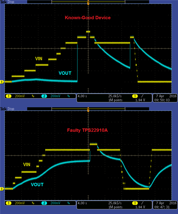
    In further investigation of this issue I have also noticed that we also have about 2.5% of parts where the UVLO behaves differently to other units.  On a typical unit from this reel with VON=0V (enabled) and VIN varied, the UVLO forces the output to GND from ~0.3V until the the threshold is passed (~0.8V on these units).  On the faulty units the output is never fully disconnected from the input and some current flows (but the switch is not turned on).

    Here is a capture of the VIN and VOUT.  There is some load on the output as it is still connected to the rest of our circuit.  You can see that on a good device the TPS22910A output is disabled, and no current flows.  However, on the faulty devices the output is not fully disabled, and there is some very small current flow.

  • Hi Adam,

    On the faulty devices, do you know how much current is flowing from VIN to VOUT?  Also, do you have an estimate of the capacitance and load on the output of the TPS22910A?

    The reason I ask is because I would like to try and replicate this issue to see what I get in the lab.  I may not be able to perform the exact input waveform seen in the scope shots, but I could at least monitor VOUT for various levels of VIN.

    In general, the TPS22910A does not have any quick output discharge.  When the UVLO kicks in, it does not force the output to 0V, it just leaves the output floating.  The discharge rate of the output capacitor is dependent on the system load.

    Thanks,

    Alek Kaknevicius

  • Hi Alek,
    I have been looking more at the devices. What I have seen is that we are seeing multiple failure modes.  Some I believe can be attributed to soldering issues or mechanical damage.  However, for a number of them we have been unable to find any form of damage despite visual inspection, x-ray and cross-sectioning. The parts have underfill and conformal coating due to the flexible nature of our PCB.  We have used TI DSBGA packages extensively in the past.

    There is one fault we are seeing that I am particularly concerned about.

    The circuit is as shown above.  The purpose is that there are two power sources, batteries (BATT: 2.0V - 3.3V nominal) and an external power connector (VPROG: 3.0V nominal).  Either or both may be present, and VPROG takes precedence.  The circuit is such that if either BATT or VPROG are present, but not the other then that will be connected to VSYS.  If both are present, VPROG will be connected to VSYS.  If both are present and VPROG is removed, the system will swap to BATT once VPROG (and VSYS) decay to a low enough voltage.  Because of the slow turn-on time of IC309 and fast turn off of IC300, there should be a time period where both switches are off.

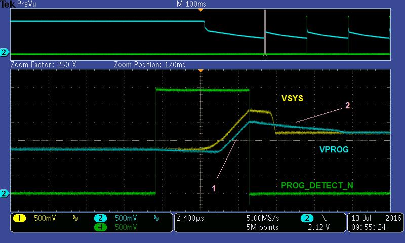
    The circuit works as expected on most devices.  However, on a small number of devices (~3%) we see a fault where the the reverse current protection in IC300 is not functioning correctly.  On these devices, when VSYS ramps up from connecton to BATT, VPROG also follows VSYS.  VSYS rises above the threshold of IC310 and the circuit swaps inputs.  This can be seen in the waveform below.  This oscillation keeps happening, and the device thus never powers up.

    This does not match what I expect to happen for the device, as you can see that at point (1) EN* =High, VIN>1.5V, and the VRCP and TDELAY parameters have been met but the switch is still allowing reverse current.  Additionally, at (2) the switch, which should be fully on does not appear to be on.

    On a fully functional device, we see the following:

    Here you can see that IC300 is blocking any reverse current as expected.

    My initial thought was that perhaps there is a soldering issue on the part, on either the GND or EN* balls.  However, I have not been able to confirm that on many parts.  Do you have any other thoughts or suggestions?  Is this an invalid way to operate this IC?

  • Hi Adam,

    Apologies for the late reply here.

    I took a look at your circuit with another engineer and neither of us saw anything which seems to be a large concern here.  We would like to try and replicate this circuit in our lab as well as potentially simulate this design to see if any issues are present.  The only other question we have is what rail is powering the SN74LVC2G14? 

    Our current plan is to get back to you next week with some results.  Would that be acceptable?

    Thanks,

    Alek Kaknevicius

  • Hi Alek,

    Thank you for your assistance.

    The SN74LVC2G14 is powered by the BATT supply.

    I am increasingly thinking that on some units there is an open circuit on the EN* or GND pins that is not visible.  I have noted that on a number of units the frequency that it oscillates between the states can be changed by placing a hand close to the device.

    Unfortunately I am not able to replicate this behaviour using an evaluation board.  However, I believe the one I have is very old as the IC markings do not match the markings specified in the datasheet.

    Adam