This thread has been locked.

If you have a related question, please click the "Ask a related question" button in the top right corner. The newly created question will be automatically linked to this question.

TPS54331 failing

Other Parts Discussed in Thread: TPS54331

HI,

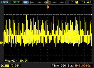
I have attached my schematic and layout. This is regulating 5-18V down to 5V to power the rest of my circuit.Preteckt_sch2.0.pdfIt works well during testing but after letting it run for more than an hour, it unexpectedly shuts down. with 12V VCC I get 200mV out of the TPS54331.

Now the first time this happened I thought it was dead, but after a few hours of letting it sit un-powered, it starts working again the next time you power it up. Then after 45ish minutes it shuts down again.Preteckt2.0.pdf

Does anyone have suggestions? On why this is happening?

  • I do not see anything in the schematic that jumps out at me. When the IC is operating, does the case get hot? Can I see the PCB layout?
  • Nope, no heat. It only happen when the Pi is being powered though- Its drawing 130-150mA when this is happening.

    The poured version is attached in my original question. A poured version is now attached also

    5584.Preteckt2.0.pdf

    Thanks

  • I am not sure what the cause of your shut down is, but I can tell you there are quite a few issues with the layout. Basically, you need to have more direct top side GND path. To achieve this, you need to route the BOOT cap trace on the back side. See the datasheet layout guidelines on sh.25, fig. 25. Poor ground routing of the catch diode and Vin capacitor are always problematic as well as routing the FB trace under the inductor. To troubleshoot your issue will have to instrument your circuit and wait for it to shut down. I would monitor PH and Vout to start with. Trigger on Vout dropping out and examine the PH signal at that time.
  • John,

    Thanks for the reply. I have tried again at laying out my board. A picture is attached. Do you think that this failure is an inductor or diode problem? I really don't see what else could be the issue. When the failure happens there is 1.1V on pin 8

    4527.Preteckt2.0.pdf

  • The layout looks quite a bit better.  I would move C1 closer to the IC.  I would swap location of C4 and D2.  I would connect the FB trace near C3.  You can rout it on a different layer to get it away from L1 and the SW node.  I typically do not even place GND fill directly under the inductor.

    I would need to see waveforms to comment further about your device shut down.

  • Thanks for the help with the layout. When you say you need waveforms are you saying you need them of the actual second of failure? Right now with a supply voltage of 13.5V the voltage on the pins are as follows

    pin 1 - 800mV                                     pin 8 - 1.2V

    pin 2 - 13.5V                                       pin 7 - 200mV

    pin 3 - 1.2V                                         pin 6 - 800mV

    pin 4 - 200mV                                    pin 5 - 400mV

    waiting a few minutes I get a sudden burst where it looks like its trying to power back on and I get the following waveform on pin 8. Second later its back to the failure with 1.2V on pin 8.

    Do you think the inductor needs to be changed?

  • Generally speaking, dc voltage measurement of the pins are not very helpful for troubleshooting.  I can't really tell what is going on in the waveform as the timescale is to long.  It needs to be 10 usec/div or so.  Ideally you should trigger on the voltage dropping out so I can see what is happening immediately before and after the drop out.