This thread has been locked.

If you have a related question, please click the "Ask a related question" button in the top right corner. The newly created question will be automatically linked to this question.

BQ25504 Vbat_ok low on changing Vin_dc

Other Parts Discussed in Thread: BQ25504

Thanks in advance for any insight - I'll start with the relevant programmable settings:

  • Vbat_ov - 4.149V
  • Vbat_ok - 3.128V
  • Vbat_ok_hyst - 3.280V
  • Vbat_uv - 3.085V

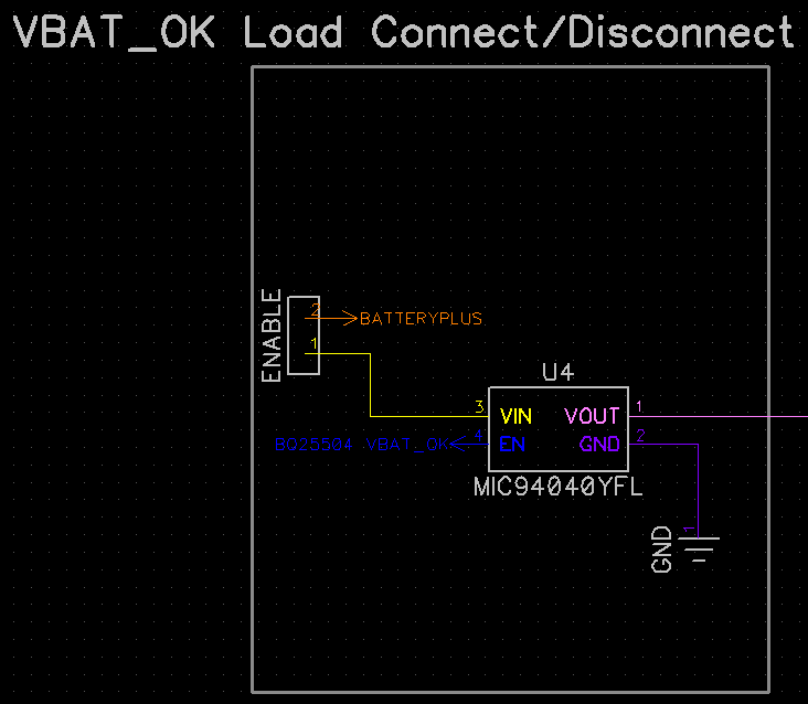
I'm using a solar cell with Voc = 2.52V and Isc = 150mA (MPP 2.0V and 133mA) and a 3.7V 2200mAh Li-ion battery as the storage element. I found out after the original design of the board that BQ25504 can't source the load transients from the load over the Vstor -> Vbat FET and have instead sourced the load from Vbat using the Vbat_ok signal to control an external PFET (this is a separate issue altogether but potentially relevant). 

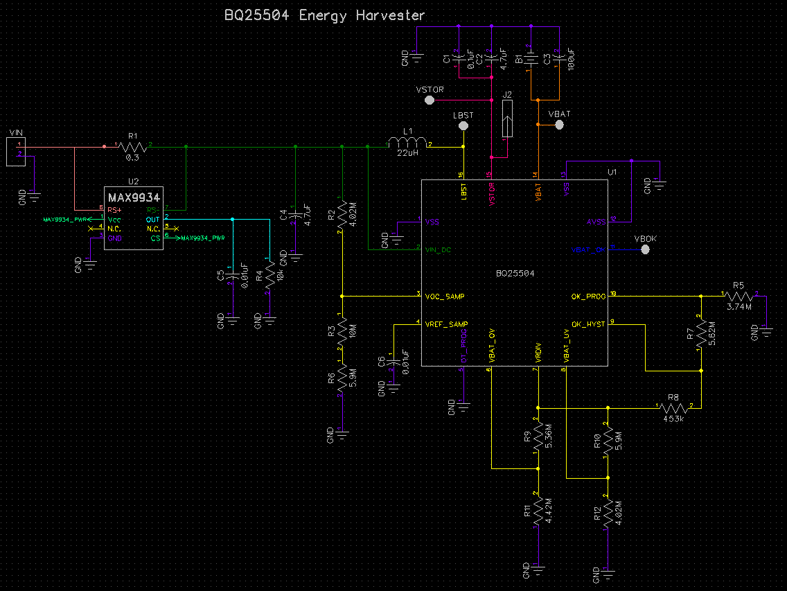
The schematic for the BQ25504 circuitry:

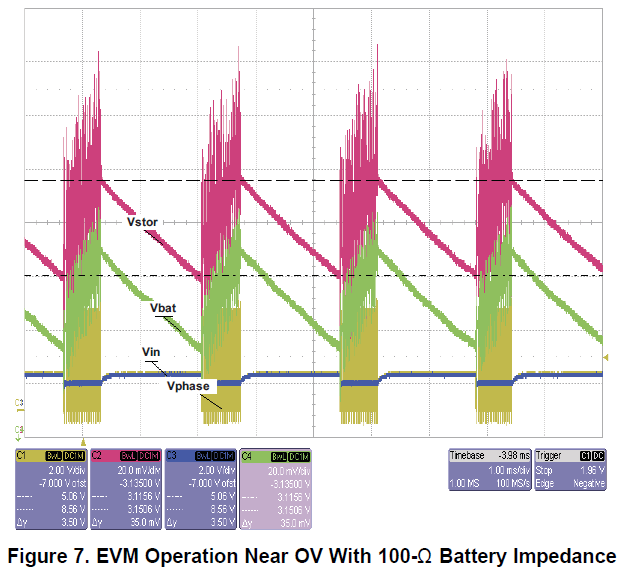
The problem I'm seeing now is that when the solar cell input varies quickly and/or drastically (e.g. a cloud moves overhead on a sunny day), I will sometimes lose power to my load. I recreated this setup in the lab and by moving an object between the light source and the solar cell I can see that the Vbat_ok line is actually dipping low although the Vbat and Vstor lines do not dip at all. I'm wondering what could possibly be causing Vbat_ok to drop low - attached is the scope output of this occurring where the scope lines are as follows:

  1.  Vbat_ok (yellow)
  2. Vstor (blue)
  3. Load (pink)
  4. Vin_dc (green)

I didn't include the Vbat line on this scope but have verified that during this condition the voltage on the battery doesn't budge.

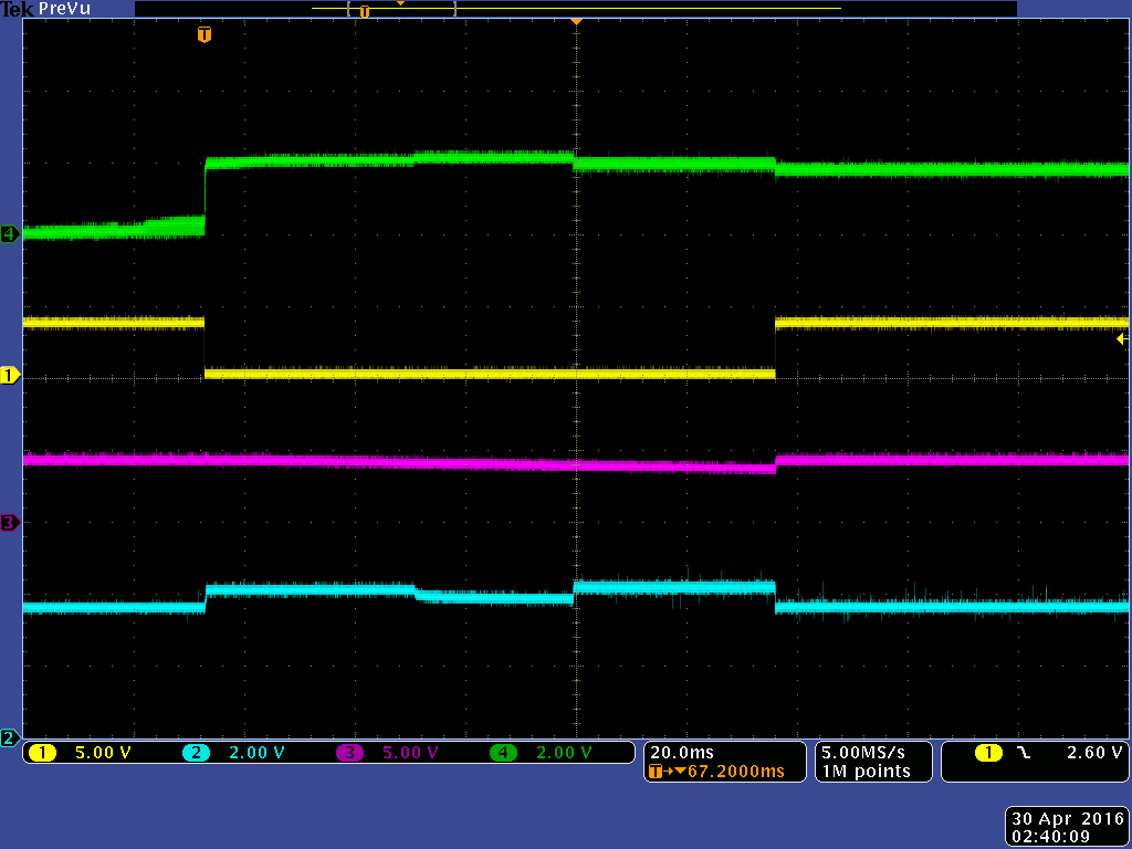
The Vbat_ok line consistently stays low for ~100ms every time this occurs. Fortunately in the lab the input capacitance on the load keeps the voltage high enough to continue operation but on my test setup that is outside I'm logging about 5-10 restarts a day where the load capacitance isn't enough to keep the load powered. Anyone have any thoughts as to how to prevent the Vbat_ok line from dipping?

In the case it helps, here is the schematic of the external PFET:

Thanks!

  • Just a follow up - I'm realizing that this condition happens when the battery is near the OV condition. 

    In the EVM documentation it shows a wave form for when this condition occurs - there is ~35mV drop before the boost converter comes back on. Figure 7 in the datasheet (shown below) doesn't include the Vbat_ok signal.

    To recreate this I'm using a 3.7V li-ion battery with a PS hooked up to Vin and sweeping (albeit manually and rather poorly) from 0v-2.0v. The resulting waveform is:

    Where the waveforms are:

    1. Yellow - Vbat_ok
    2. Blue - Load
    3. Pink - Vphase
    4. Green - Vin

    The battery voltage is just around the OV condition (fully charged) and my load is being controlled by the Vbat_ok signal (via an external PFET). I ran the same test with a battery that was only charged about half-way and the Vbat_ok signal remained high throughout the entire Vin sweep:

    My question then is what can I do when the battery is near the OV condition to keep the load attached since Vbat_ok is dropping low and occasionally forcing the load to restart? The Vbat_ok low consistently lasts 100ms so would the solution be to put a capacitor on the Vbat_ok line to keep the voltage controlling the external PFET high long enough to avoid the OV condition?

    Any help is greatly appreciated, I've been trying to figure out what exactly is happening for way too long now. Thanks!

  • JD,

    Just so I understand, do you still see this behavior when the VIN not present? Could you try connecting a DC supply at VBAT(with decent current compliance) and then see if you can duplicate this issue? (tricking VBAT to be close to VBAT_OV and avoid any sharp transients from the load)

    What is the profile you turn on the load from? Have you tried additional capacitance on VBAT? I typically dont like adding too much capacitance on digital signals as it could potentially mask a real scenario. (we will keep this as a last step)

    regards,
    Gautham
  • Gautham,

    Thanks for the reply.

    This behavior only occurs when VIN is present and the boost converter is on. If the battery is near OV and the boost converter starts up, it would make sense that the OV condition is met and I assume that this is what causes the Vbat_ok line to go low but I still need my load to maintain operation.

    As you suggested, I tried hooking up a DC supply to VBAT at 4.05V (my Vbat_ov is set to 4.149V) and sweeping VIN. The same behavior occurs and the scope output is below:

    1. Yellow - Vbat_ok
    2. Blue - Load
    3. Pink - Vphase
    4. Green - Vin

    The load goes to to two TPS6300x buck/boost converters (3.3V and 5V). The 3.3V is provided to an on-board MSP432 and the 5V goes to an external load. The external load draws 170mA-250mA at 5V on startup for ~250ms and then during normal operation the external load consumes about ~200uA.

    There is an added external 100uF capacitor in parallel with VBAT.

    Also, good call on not adding the extra capacitance to the digital line - I had tried it out of desperation prior to your response and it didn't work out.

    Thanks!

    JD

  • Delayed update but I tried hooking up an evaluation board to my load to make sure it was a problem with my PCB design. This worked fine so I started looking for differences in my layout for the BQ25504 and the evaluation board. Turns out I didn't attach the PowerPad to ground - unless I'm missing something, other than section 11.1 and 11.2 in the BQ25504 there isn't mention of the PowerPad so I must have just missed the importance of having to tie it to ground.

    The BQ25504 eval board datasheet says in section 4.4:

    4. It is critical that the exposed thermal pad on the backside of the bq25504 package be soldered to the PCB ground. Make sure there are sufficient thermal vias right underneath the IC, connecting to the ground plane on the other layers

    In the layout guidelines, there are 9 vias under the exposed pad and I was wondering what would be considered sufficient and would anyone happen to know the hole diameter and outer diameter of those vias? Also, do those vias need to be filled and if so, should the fill be conductive?

    Wish I would have caught this sooner but at least everything seems stable now. I tried a proto PCB without the thermal vias under the BQ to keep the cost down and the issues I previously mentioned seem to be resolved. Based on 4.4 mentioned above it seems like having Vias-In-Pad are pretty critical as well and I assume it's all about thermal dissipation. Can anyone provide some more information on this?

    Thanks!

  • JD,

    I am glad that you got to the root cause of the issue. The vias on the QFN pads are there to let excess solder to flow to the back side of the board during reflow. 

    You dont have to fill those vias up. (It might actually be bad for your board) I do via fills for WCSP/ BGA devices usually. 

    I would reuse the same drill size you used else where on your board. (35mil outer- 25mil inner or so)

    The via fill is an expensive process. You don't need that here for this IC. 

    regards,

    Gautham