This thread has been locked.

If you have a related question, please click the "Ask a related question" button in the top right corner. The newly created question will be automatically linked to this question.

TPS63020 Power save disabled, instability when Vin=Vout

Other Parts Discussed in Thread: TPS63020

Hello everyone,

I'm experiencing some trouble with TPS63020 when the input and output voltage are equals (+/-0.4V) in power save mode disabled.

I explain : When the input and output voltage are far from each other, lets say Vin=2.4V and Vout=3.5V, then the buck boost is working nicely. But when these two voltages are close to each other then I guess the buck boost is switching between buck mode and boost mode.

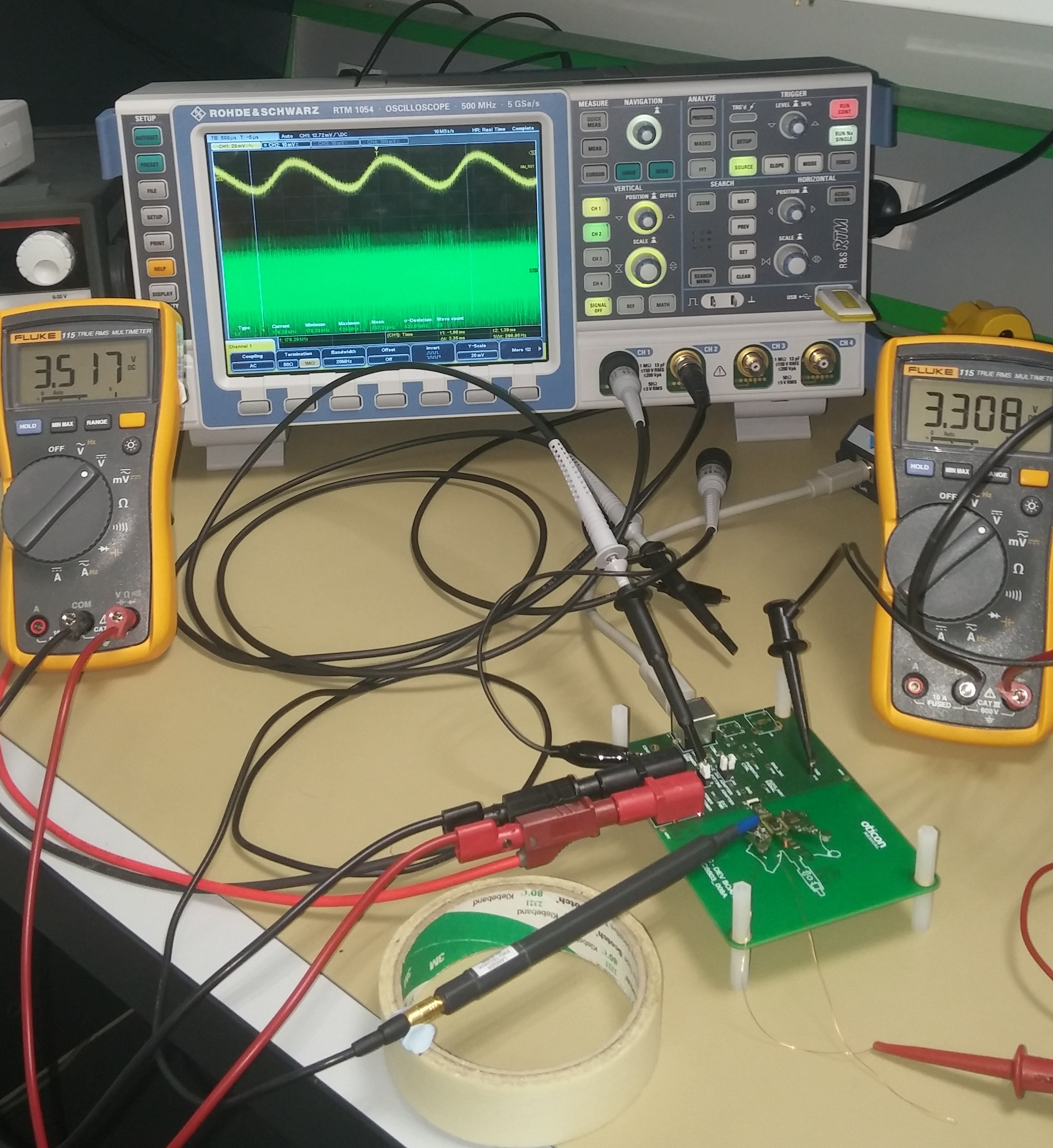
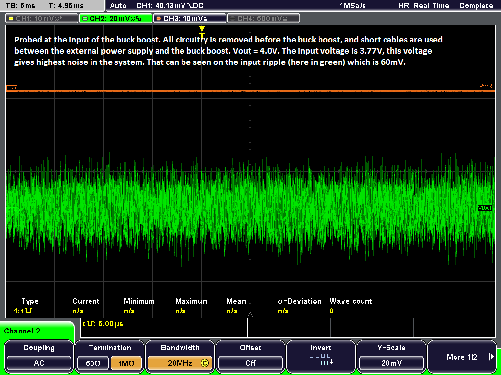
This oscillation can be seen on the input voltage : a slow ripple frequency of ~700Hz, with 30mV amplitude. When regulator switch between one mode to the other, it creates high current surges in the switching coil. These current surges create a magnetic noise that disturb a low power inductive link..

I have made some screen shots of the problem : (left is okay, right is the problem) The red circle show the repetitive magnetic noise.

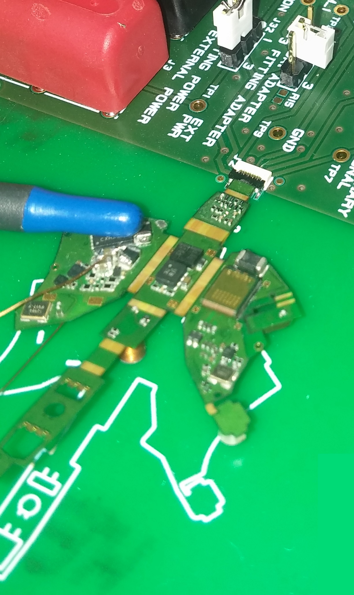
SCM and is below, I cannot show the PCB but the routing is very direct and I don't think the routing can help here.

I can see this issue for a Vin=[1.8V to 4.2V] The problem is worse when Vin is high. The loads are from [10mW to 100mW].

With and without the input ferrite bead is the same, the frequency is very low anyway. I think that more decoupling at the input won't help for the same reason. There are 100µF more at the input (low ESR tantalum capacitors).

If you have any idea to reduce the impacted voltage range from +/-0.4V to +/-0.2V that would already help a lot. I wonder if we can make this problem disappear at all as this oscillation is part of the good voltage regulation of the regulator.

Any other idea? :)

Thank you in already for reading !

Best regards,
Martin

  • Can you please share a picture of your measurement setup?
    Can you also provide a scope plot of Vout and the switching nodes when you see these oscillations?
  • Hello Sabrina and thank you for your answer.

    Below I have remade the measurement and zoomed on the two parts of the oscillations (when Vin is higher than expected and when it is lower). The added noise is due to the coupling of the oscilloscope channel : the L1 and L2 channels are leaking on the other measures... (no noise when L1 and L2 are disconnected from the oscilloscope).

    Added comment : Vout behavior is normal in any case, no oscillations. The efficiency is not impacted by the oscillation of Vin, it remains within the specifications.

    I have also attached the test setup with the near filed probe. It is the blue tip at the left of the picture. I have placed it just over the switching coil, and over the buck boost.

    Let me know if you need more information.

    Thank you and best regards,

    Martin

  • Hello Martin,

    To summarize (correct me if I am wrong):

    1. Vout and efficiency are as expected

    2. When Vin is close to Vout,  you see oscillations according to the picture on the first post -

    • how are you powering your the buck-boost converter? These oscillations may  be caused by your measurement setup, like the cable you use to power the board, that's the reason I  need a picture of your complete measurement setup.

    3. On your second post I don't see the same kind of oscillations waveform as in your first post.

    • You mention " the two parts of the oscillations (when Vin is higher than expected and when it is lower)" - do you mean the max and min of the oscillation? this is not clear to me.
    • As L1 and L2 are causing noise, no need to connect them for the next measurements (for your information here is an app note explaining how to properly measure switch nodes : http://www.ti.com/lit/an/slva494a/slva494a.pdf).
    • It would also be nice to have on the scope plots the values of Vin and Vout  

    4. I would really like to take a look at your layout for the power stage. Can your share the different layers in PDF format?

  • Hi Sabrina,

    1. Yes

    2. Yes

    I am powering the device with an external power supply, 3.5V and current limit 400mA. I have tried short cables (30cm) instead of the long ones I used previously and the oscillations are the same.

    I forgot to tell about the power management system. There is a load switch just before the buck boost. It enables or disable the power to the buck boost.

    When considering the wires, load switch and PCB copper traces I estimate to max 3 Ohms (and that's conservative, I think it's less than that :)) the resistance between DC power supply and the buck boost. (below a full picture of the test setup).

    There are also 2x47µF tantalum capacitors (Kemet - T529P476M010AAE200) + 2x10µF ceramic capacitors (Taiyo Yuden - LMK107BJ106MA-T) at the input of the buck boost.

    3. It is zoomed a lot (time base is , so the oscillations looks flat. I have zoomed at the moment when the oscillations is high and low. Be careful it is AC voltage that is measured.
    (woops it seems the link is not working today...)

    4. The 4 layers are attached now

    Let me know if you need further information.

    Thank you and BR,
    Martin

    153549R3-22-02-2016_L1__03_2_153549.pdf153549R3-22-02-2016_L2__03_2_153549.pdf153549R3-22-02-2016_L3__03_2_153549.pdf153549R3-22-02-2016_L4__03_2_153549__03_2_153549.pdf

  • The TPS63020 regulates properly at the output, so I think this issue is related to the circuitry placed ahead of the converter. Of course in the buck-boost region the converter switches between buck mode and boost mode and pull more current when switching back and forth, but these oscillations can also be the result of a weak path for power supply therefor:

    1. Can you try to bypass the load switch and all the circuitry in between and power directly the converter? 

    2. Can you measure the input voltage directly at the input of the converter (not at the J32 jumper)?

    By the way here is the link for the app note : http://www.ti.com/lit/an/slva494a/slva494a.pdf

    I would like to share an additional comment for the layout:  the input capacitor are not placed on the same layer as the converter, this is not recommended. If you plan to do a redesign I would definitely place at least one input cap on the same layer and close to the input pin of the converter

  • Hello Sabrina,

    Sorry for the long silence, I was in holiday. Now I'm back and I've reperformed the measurements.

    First weird phenomenon, I cannot reproduce the sinusoidal oscillations shown above. Now the input ripple looks either clean or erratic - switching between buck and boost mode. I have attached a comparison of the voltages at the input of the load switch and at the input of the buck boost.

    I have also tried removing all circuitry before the buck boost. This doesn't remove the phenomenon.

    When I had removed all circuitry before the buck boost I have tried adding serial resistors between the buck boost and the external power supply. The bigger the resistor, the higher the ripple and the noise. So I agree that any resistance on the power path needs to be reduced. But I don't think I can reduce it more in our application.

    I have also tried to decouple with small capacitor values (100nF) the input voltage to remove high frequency noise but that doesn't help at all.

    I have measured the input ripple voltage for a fixed output (4.0V) in two configurations : in blue 0 Ohms between buck boost and power supply; and in red 5 Ohms between buck boost and power supply. The results are shown in the graph below :

    In short:

    - it can be seen that when vin=vout +/- 0.4V there is an increase of the input voltage (which is directly related to the magnetic noise created in the switching coil, which is normal because it is related to the inrush current) 

    - Whatever the input resistance, their are 2 main "clean bands" where the buck boost doesn't create big noise (on the picture below: #1 and #2)

    We think of an algorithm where we always control the output voltage to be outside this +/-0.4V voltage band (always higher). This is the safe solution, but it implies a big energy loss as this voltage is used for a power amplifier => a small offset mean a big loss :(

    I now think we could allow Vout in clean band #2 to lower the offset, what do you think of that? Risky? trustable? ...

    Do you think we can rely on the fact that this "clean band" will exist no matter what the output voltage (power consumptions are between 10 and 200mW)? If you have more information about the internal regulation circuitry of the IC, I would like to read that. For now I have the datasheet only which tells : "When the input voltage is close to the output voltage, one buck cycle is always followed by a boost cycle. In this condition, no more than three cycles in a row of the same mode are allowed. This control method in the buck-boost region ensures a robust control and the highest efficiency."

    I look forward hearing from you, and if you have any idea, feel free to comment.

    Best regards,

    Martin