This thread has been locked.

If you have a related question, please click the "Ask a related question" button in the top right corner. The newly created question will be automatically linked to this question.

LM5106 power dissipation: what is the capacitance CL to use in the formula?

Other Parts Discussed in Thread: LM5106

Hello all,

Just asking in regards to the formula for the power dissipation losses given in the datasheet of LM5106 (page 14), rough power loss estimate:

the question is, what is the value of CL to consider? is CL the input capacitance of the MOSFET I am trying to drive?

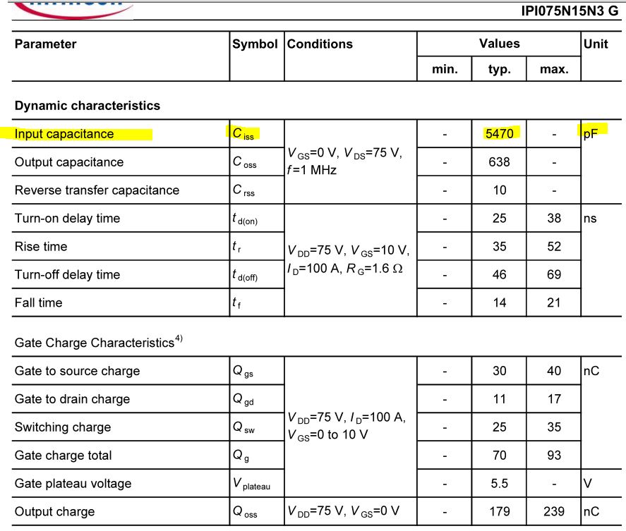
For instance I am driving the MOSFET IPP075N15N3 with the below data (the input capacitance is Ciss = 5470pF). Should I use this value Ciss to insert in the formula for the gate drive loss estimation? In other words is the load capacitance of the gate driver the MOSFET Ciss?

If you know any rule of thumb or a rough estimate to use the formula above it would really help,

Thank you very much.

Leo


  • Leo

    In the equation above, CL is the driver output load capacitance, this is stated in the previous line in the datasheet. And you are correct, this is effectively the external FET capacitance.

    However, Ciss is probably not a good figure to use. Ciss is a small-signal capacitance measurement at zero DC-bias and 1-MHz test frequency.

    When the gate capacitance is charged, the capacitance changes with applied DC-bias voltage, so again it's difficult to put a simple CL value into the eqn above.

    And the gate input capacitance is not the only relevant capacitance, there may also be Miller capacitance to charge and discharge, depending on whether the half-bridge stage is hard or soft-switched.


    To get a conservative estimate, I would recommend using the Total Gate Charge figure Qg(tot) in the datasheet instead. For the device above, Qg(tot) is 70 nC typ, 93 nC max.

    Since Q = C*V, the power dissipation eqn can be re-written as

    Pd = 2 * f * (C*V) * V = 2 * f * Q * V = 2 * 100k * 93 n * 10 = 186 mW for 2 similar half-bridge FETs switched at 100 kHz.

    Q needs to be determined at the Vdd level being used, the figure above is 70 nC typ @ 10 V, and it will vary at different gate voltages.

    Alternatively, the Qg(tot) 70 nC typ @ 10 V can be viewed instead at ~7 nF of average capacitance, and CL = 7 nF typ used instead in the original equation. This will work ok as long as Vdd is close to 10 V. If not, the Qg(tot) at the voltage of interest should be determined from the FET datasheet.

    Note that the factor of "2" in the equation is valid if both half-bridge FETs are similar part number/type. If not, the gate charge or equivalent capacitance of each FET need to be summed.

    I hope this helps answer your question. If so please click on the green "verify answer" button.

    Thanks,
    Bernard
  • Thanks Bernard your answer really helps!

    All that is left then is to estimate the Qg(tot) for the switch, as in fact as you say the datasheet  IPP075N15N3 gives this parameter at 10V only. I assume the gate driver  LM5106 is driving the gate at 12V, so I can use the Vgs vs Qg curve in the switch datasheet to determine Qg. Or put simply, since the Vgs vs. Qg dependence is linear, if Vgs=10V --> Qg=70nC, then Vgs=12V-->Qg=70e-9*(12/10)=83nC. I hope this makes sense.

    Best Regards

    Leonardo

  • Leonardo

    Yes, what you propose above is correct, from Fig. 14 in the FET datasheet, you can extrapolate linearly to estimate the total gate charge at 12 V to be about 83 NC.

    Thanks,
    Bernard