This thread has been locked.

If you have a related question, please click the "Ask a related question" button in the top right corner. The newly created question will be automatically linked to this question.

TLV62130 MOSFET Failing

Other Parts Discussed in Thread: TLV62130

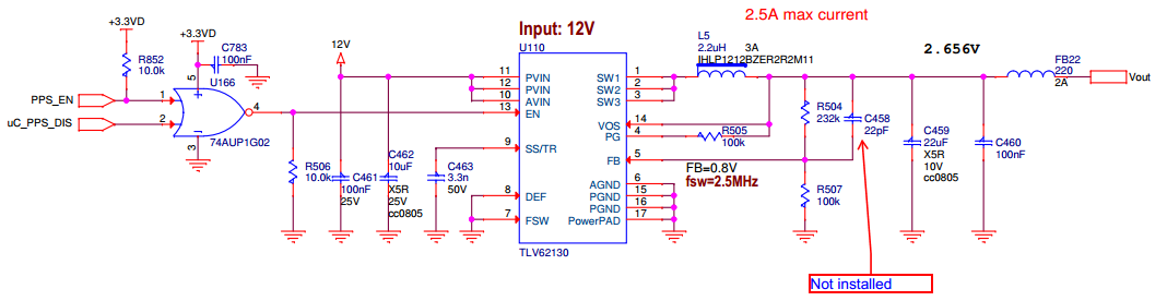
Customer has designed in a TI TLV62130 DC-DC converter for a line card project. They are currently having some failures where the bottom MOSFET is failing short at about a 10% rate on the prototype line cards. The device is being operated well below its maximum specified current – it is operated at about 1.5A max, 2.5V output, and it is rated for 3A. The device is rated for a 17V maximum input, and we have a well regulated 12V input. The basic design follows the data sheet recommendations.


We would like to know if there are any known issues with this part, specifically the MOSFET short failure that we are seeing, and if there is any recommendation from TI concerning use of this part. We are planning on going into the second prototype phase soon, and we don’t have a plan for moving forward.  


We are using the TLV62130 (not the “A” version), the schematic is attached. The part number for the inductor is on the schematic, and the other passive components are generic R’s and C’s. Other than the 0805 10uF and 22uF caps, all other R’s and C’s are 0402.


  • As far as power supply failures go (which are not particularly common), a SW to GND short as you have is the most common one. This is usually the result of PCB layout errors. an you post your PCB layout and part numbers of C462 and C459?
  • I've attached the layout. The board is 10 layers, with 2 ground layers and 2 power layers.

    Part numbers:

    C459 – TDK C2012X5R1A226K125AB

    C462 – AVX 08053D106KAT2A

  • Thanks for posting.

    There is a major error in the layout, in that, the 10uF input cap connects to the AGND side of the IC and not the PGND. This adds impedance to the switching currents which can overstress the IC. See the D/S layout example for a proper layout.

    As well, they should add thermal vias under the IC to cool it. I don't think the thermal performance is very good with the current layout.

    As well, R504 should move over next to the FB pin to keep that net small. Finally, move R506 anywhere else. It's in the way and not critical to the circuit.

    You can post the new layout here and I can review it.

    As well, the AVX input cap is just in an 0805 package. This is pretty small and will have significant DC bias loss. Do they have a DC bias curve from AVX? I could not find one. They likely need to use a bigger package one or 2 in parallel.