This thread has been locked.

If you have a related question, please click the "Ask a related question" button in the top right corner. The newly created question will be automatically linked to this question.

BQ78350-R1 technical reference manual

Other Parts Discussed in Thread: BQ78350-R1, BQ76930, BQ76940, BQSTUDIO, BQ78350, BQ76930EVM, BQ34Z100-G1, GPCCEDV, BQ76940EVM

Hi all

My company is developing a BMS solution using the BQ78350-R1 and the BQ76930. I am on charge of the "golden image". The BQ78350-R1 technical reference manual (TRM) show all the registers in the BQ78350-R1. Unfortunately, I could not find detailed explanation for each bit on several registers on the TRM or related documents.

Could you let me know where to find detailed explanation for each bits and registers of this chip.

Thanks in advance

  • Dear Julio and colleagues,

    Did you find the register map for the BQ78350-R1? I am also using the IC and I could not find well desribed register map like the one of BQ76940.

    Information for the register and functionality will be highly appreciated.

    Thanks
  • The data in the TRM is the only documentation that we have for the bit definitions. If you have questions about specific bits or features, then let me know and I will try to clarify.

    The best place to find that register map is in the Data Memory section of bqStudio. There were a couplr address errors in the TRM and I am not sure whether they have been corrected.
  • Dear Krasen and Thomas

    Thanks for your reply. Yes, the Data Memory section of bqStudio shows the Register Map; Krasen, did you have activated the "Show Advanced Views" on Battery MAnagment Studio? you can find it at Window>Preferences>All Global Settings and then set the "Show Advanced Views" check box.

    Thomas, as you mentioned that the only documentation available is the TRM, I am going to continue the golden image developing and I will let you know if doubts appear.

    Question: DA Configuration [IN_SYSTEM_SLEEP] bit is used to get communications when the BQ78350-R1 is in SLEEP mode, what is the use case for this feature?

    Do I have to press "Verify Answer button"? and then continue in this link for future questions?
  • Hi Thomas

    I am making some test on the calibration stage of bqStudio. In the Voltage section,

    1.- The bq78350 TRM mentions that "New Ext Cell Divider Gain" = (Old Ext Cell Divider Gain × Actual Avg Cell Voltage)/Measured Avg Cell Voltage. Where can I find "Measured Avg Cell Voltage" value?

    2.-The bq78350 TRM mentions that "New VAUX Gain" = (Old VAUX Gain/VAUX Voltage). Is the "VAUX Voltage" value on mV units?

    Thanks in advance

  • Dear Julio dear Thomas, 

    My colleague told me that he found the Register Map in bqStudio software but he couldn't find any information for each of the register and what can be done with each of it. Can you please help me with this issue. 

    He needs something which is similar to this file    Please check on page 33 . 

    Thank you in advance! 

    With best regards,

    Krasen Mateev

  • If you do not see the address, etc for each prameter, then go to Window >> All Global Settings and select Show Advanced Views. The information should then be available. The bq769x0 registers are not available in bqStudio.
  • Hi Thomas

    I am working on the BQ78350 register configuration. In the TRM page 65 the document mentions that EDV detection is disabled when Fuel Gauging: CEVD Cfg: Overload Current threshold is reached; then, BQ78350 resumes EDV threshold detection after C drops below the Overload Current threshold.

    I would like to ask for the threshold for Fuel Gauging: CEVD Cfg: Overload Current, I think that this current have to be between system maximum discharge current and the current threshold set in OCD (or any) protection, is it correct?

    system maximum discharge current < Fuel Gauging: CEVD Cfg: Overload Current OCD: threshold < AOLDL: Threshold and Delay

  • The OVerload current does need to be set above below the protection current thresholds. It should be set above the maximum discharge current. You chose a maximum discharge current when you collected the log files to calculate the CEDV Coefficients. The gauge uses these coefficients to simulate the discharge profile and the purpose of the Overload current is to disable the EDV detection if the current is much greater than the maximum current used to calculate the coefficients.
  • Hi Thomas

    Thanks for the reply, now it is clear to me.

    Actually, I am going to start the discharge profiles suggested in the "Simple Guide to CEDV Data Collection for Gauging Parameter Calculator (GPC)" document. Is it correct to keep active the CEDV compensation and leave the default EDV coefficients during discharge logging?

    Thanks in advance
  • Hi Thomas

    My project leader ask a question: "Has Texas Instruments the CEDV coefficients for our cell and battery pack configuration?". Our application is an E-Bike power train (0°C-50°C operational temperature range) and we are using the ICR18650-22P cell from Samsung. The battery pack is a 10s3p configuration. The cell we are using is very standard and it is included in the chemistry catalog that comes inside the bqStudio 1.3.52. It would help us very much and save us considerable time if we could avoid the step of sending the discharge profiles of our cell/battery pack. 

    Thanks in advance

  • Julio
    We do not have CEDV coefficients for various cells. The profiles should be run on your specific cell configuration to get the best results.
    Tom
  • Hi Thomas

    Thanks for your reply. I am going to start the discharge profiles as suggested. Is it correct to keep active the CEDV compensation and leave the default CEDV coefficients during discharge logging?

    Thanks in advance

  • Yes, we are just interested in the time, V, I , T data in the log file, so gauging parameters will not be used.
  •     Hi Thomas

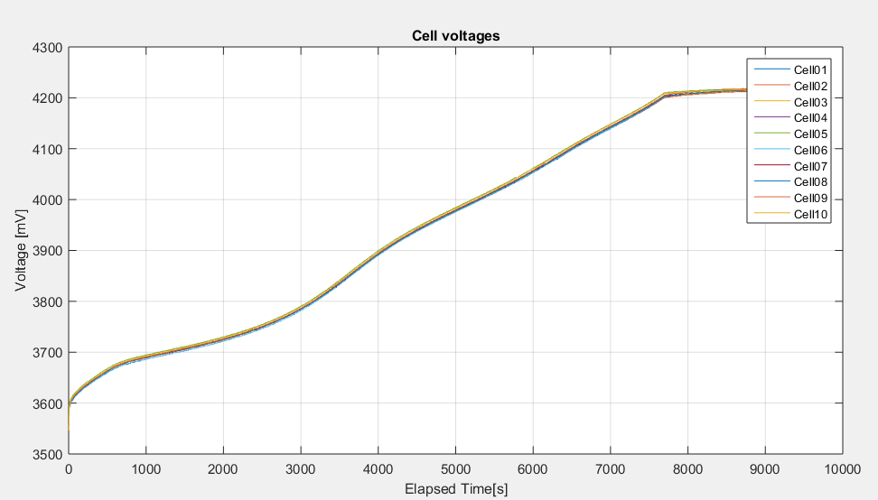
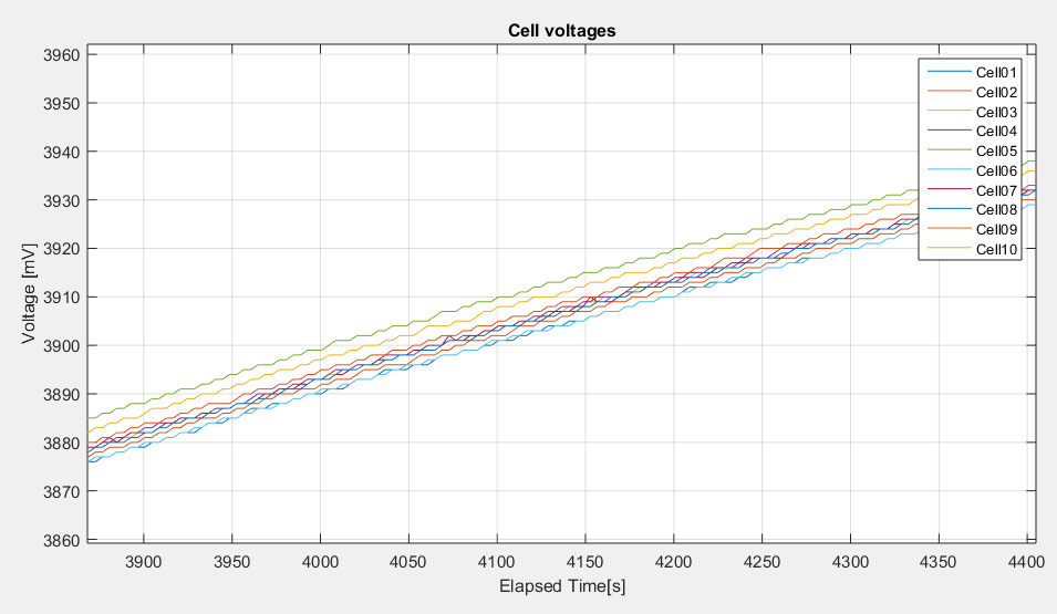
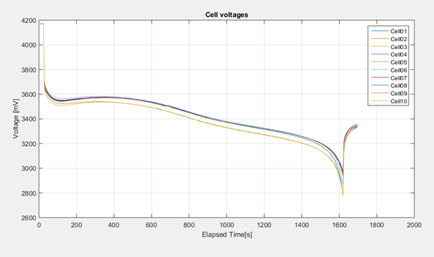
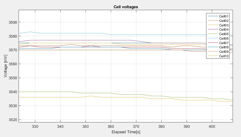
    We are generating the discharging profiles and start to notice something. As you can see in the attached images, Cell05 and Cell10 voltages shows a different behavior respect other Cells. Their voltage drop more during discharge mode and rise more during charge mode.

    We are using the Evaluation module bq76930EVM for charge and discharge the battery pack. The cells are new and completely balanced at the begging of the test.

    Have you seen this before? What do you think is happening?

    Thanks in advance

  • It is usually an indicator that the series resistance is higher and the cell is damaged, if a cell trends higher during charging and lower during charging. Have you measured the cell voltages with a volt meter to verify whether they are really different?
  • Hi Thomas

    I just measured the cell voltages with a voltmeter:

    Cell01: 3592mV

    Cell02: 3592mV

    Cell03: 3592mV

    Cell04: 3592mV

    Cell05: 3592mV

    Cell06: 3592mV

    Cell07: 3591mV

    Cell08: 3590mV

    Cell09: 3591mV

    Cell10: 3592mV

    What do you recommend to do in the next step?

  • Hi Thomas

    I am performing the discharge profiles for CEDV coefficients determination. My discharge rates rates are 14A and 7A at 0°C, 25°C, and 45°C; however, I expect to discharge no more than 7A at 45°C in the real application.

    Is it possible to set the hightemp_highrate and hightemp_lowrate files with the same discharge profile at 7A? or Do I must perform the test for 14A at 45°C?

  • Julio
    We recommend using the same discharge currents for all three temperature ranges.
    Tom
  • Hi Tom

    Thanks for the fast response. Another question, In TRM, section 9.1.7 Qualified Discharge: "The temperature does not drop below the low temperature thresholds programmed in Low Temp during the discharge period." I think this refers to CDEV Cfg [Learning Low Temperature] bit, is it correct? If affirmative, this value should be set before the UTP threshold, is it correct?

    Thanks in advance

  • Hi Tom

    I performed the high temperature (45°C) and high discharge rate (14A); unfortunately, this made the battery reach 70°C, which is the maximum cell temperature, then I had to terminate the test before reach the battery full discharge condition to avoid a cell damage.

    1.- Is it possible to fill the hightemp_highrate file with these data (even if the full discharge was not obtained)?

    if negative:

    2.- What do you recommend to do?

  • You can try using the lower discharge rates for the high temp data sets and we can see how the CEDV coefficients perform.

  • Hi Tom

    I used the lower discharge rate in the high temp data set. .This is the response from the Gauging Parameter Calculator Tool, What do you think? 

    GPC CEDV tool, rev=40
    Configuration used in present fit
    ProcessingType=1
    NumCellSeries=10
    CellTermV=3000
    LearnSOC%=7
    FitMaxSOC%=9
    FitMinSOC%=3
    ChemType=1
    ElapsedTimeColumn=0
    VoltageColumn=1
    TemperatureColumn=2
    CurrentColumn=3

    CEDV parameters resulting from the fit. If EDVV bit is set to 1, EMF and EDVR0 have to be multiplied by the number of serial cells when written to data flash

    EMF 3686
    EDVC0 298
    EDVC1 0
    EDVR1 1
    EDVR0 191
    EDVT0 3330
    EDVTC 9
    VOC75 39450
    VOC50 38130
    VOC25 37540


    Recommended SOC deviation tolerance at EDV2 point is < 5% for low temperature and <3% for room and high temperature

    Deviations for this set of parameters are given below for each file

    file SOC error, % pass
    roomtemp_lowrate.csv -0.866457676931629 1
    roomtemp_highrate.csv -1.66413569836987 1
    hightemp_lowrate.csv -0.162886078054486 1
    hightemp_highrate.csv -0.162886078054486 1
    lowtemp_lowrate.csv -0.773446827308947 1
    lowtemp_highrate.csv -0.120157513610947 1

    Deviations are within recomended range. CEDV parameters are suitable for programming the gauge

  • The parameters should okay. You can run with them and check the performance.

  • Julio
    I am catching up on the e2e forum. We do not have a generic set of CEDV coefficients for various cells. Unfortunately, we do not have the resources to run the characterization profiles here.
    Tom
  • Hi Tom

    I think this answer was for an old question, right now I am testing the battery pack with the CEDV coefficients from the gauging parameter calculator tool.

    On the other hand, could you answer this other old question please:

    "Hi Tom

    Thanks for the fast response. Another question, In TRM, section 9.1.7 Qualified Discharge: "The temperature does not drop below the low temperature thresholds programmed in Low Temp during the discharge period." I think this refers to CDEV Cfg [Learning Low Temperature], is it correct? If affirmative, this value should be set before the UTP threshold, is it correct?"

    Thanks in advance

  • Yes, that is correct.
  • Hi Tom

    I do not understand the criteria (% Design capacity maybe?) to fill the FCC Learn Up and FCC Learn Down setting. Is there some documentation about it?

    Thanks in advance

  • Most users leave these parameters at there default values and these are the values that we have had hard coded into our older gauges. The usage is that FCC cannot increase by more than the FCC Learn Up value (512 mAh) or decrease by more than the FCC Learn Down value (256mAh) in a single update. The updated will be clamped by this update value.
  • Hi Tom

    Related to Battery Low% register, in our application (E-Bike) the low rate discharge (7A) is expected as the current needed to reach 25km/h. After SOC goes under 10% the discharge rate will change to maximum 4A; then, when SOC goes under 5% the discharge current will change to maximum 500mA.

    1.- What is the criteria to set the Battery Low% register?

    2.- According to the context showed above, do I have to keep Battery low higher than 10% or 5%?

    Related to production programming. At factory, we expect to connect a resistor voltage divider (cell simulator); then, download the latest firmware, golden image and perform the calibration process. If the voltage in the cell simulator is different than real cells voltage when they are fist attached to the HW, Is this going to be a disturbance on the FCC, RC and RSOC learning? If affirmative, Is this going to be solved immediately when full charge condition be present?

  • That BATLOW feature monitors the effective cell voltage and sets the flag after the cell voltages drops below the Cell BL threshold for the Cell BL Voltage TIme. You may want to use the SOC1 and SOCF flags instead. They will set when Remaining capacity drops below their respective thresholds near the end of discharge. They are not tied to SOC%, but they can monitor capacity.

    You are calibrating the voltage divider network, so using a resistor divider to voltage is acceptable. The gauge should still measure the cells with the same accuracy after they are attached. It will not have a negative affect gauging accuracy.
  • Hi Tom

    Thanks for the quick response. After checking the E2E forum, I found a link that is similar to our application behavior:
    e2e.ti.com/.../1662552

    If we obtain the CEDV coefficients with high discharge rate of 14A and low rate discharge rate of 7A, could we obtain an accurate SOC% when the discharge current is below the low rate?

    My main concern is that we are displaying the SOC, we do not want to display, lets say, 18% and suddenly 7%. Thanks in advance
  • Julio
    Disregard my previous response regarding BATLOW. I thought that you were referring to the bq34z100-G1. The bq78350-R1 does not have the BATLOW interrupt.

    When you run the GPCCEDV program with a 14A and 7A discharge rate profile, then the CEDV coefficients will be tuned to support discharge rates in that range. It can also support lower discharge rates, but you may lose some accuracy. If you use a lower discharge rate, then it will be more likely that it would hold at 7% rather than drop to 7%. You will have to test it to verify.

    Tom
  • Hi Tom

    I had been performing some charge and discharge test. At some point of the discharge, close to SOC= 20%, the RC is readjusted to the EDV2 value (Battery Low%= 7). These are the test results:

    Test 1 Test 2
    FCC_init [mAh] 6600 6344
    I_DSC [mA] 4850 5100
    TestTime@SOC_5% [h] 1.13 1.11
    RemovedC [mAh] 5490 5695
    SOCjump [%] 20 -> 7 18 -> 7
    RC@SOC_5%[mAh] 322 320
    SOH [%] 96 92
    FCC_learned 6344 6088
    MissingC [mA] 781 329

    This is a 6.6Ah battery pack (10s3p@Samsung_ICR18650-22P), but the BQ78350 is determining less capacity. This is a drawback to our system because more-less 10% of battery capacity is not used. 

    How do you recommend to solve this issue?

  • Hi Tom

    During the last weekend I decided to remove the CEDV compensation (EDV_CMP=0; Battery Low%= 0). After two discharge tests until the system turns off the results are as below:

    Test01 Test02
    FCC init 6450 6194
    Fcc learned 6194 6095
    SoH 96 94

    Without the CEDV compensation, the battery pack goes from 100% to 0% after two discharge test. I think that CEDV Comp is focused on constant discharge profiles such as  GPCCEDV program which is not the our use case.

    1.- What is the risk to avoid CEDV compensation?

    Regarding the Mfg Status init register, at all my test I set FET_EN=1.

    2.- Do I have to clear this bit in the golden image when it be downloaded at factory?

  • The CEDV Compensation improves gauging accuracy when temperature load conditions are changing. Fixed EDV does not help with this. You can have the FETs enabled in the golden file.
  • Hi Tom

    We have an issue related to the SOC. When I test the system at laboratory from 100% to 0% (just one discharge no relax time) the SOC and remaining capacity displayed look good. Unfortunately, when the system turns on from a relax time (lets say 12hr), the SOC displayed is greater than the SOC noted before.

    We are not implementing the CEDV compensation, only the coulomb counter must be used to update the RC registers.

    Is there another compensation capable to update (increasing without charging) the RC register?

    I will really appreciate a quick response. Thanks

  • The CEDV gauges do not run FCC simulations to update capacities due to OCV changes during rest. They will run a simulation, if a reset occurs. The RM and SOC can also increase, if there is a charge current. this current could be below the Deadband and you would not see it reported by the SBS Current.
  • Hi Tom

    Thanks for the quick response. I am really sure that there is not a reset condition during discharge operation or relax mode.

    "The RM and SOC can also increase, if there is a charge current. this current could be below the Deadband and you would not see it reported by the SBS Current."

    There was not charging condition in this test, only discharge and relax mode. The FCC learned is exactly the same as the lab test obtained, it indicates that it is not a bad calculation of coulomb counting (DCR register). We are displaying the relative state of charge value from the BQ.

    1.- Is it possible that something goes wrong in the calculation of this value?

    2.- I am attaching the golden image for our application, Could you take a look of it, in order to verify that everything is ok?

    * Texas Instruments Data Flash File
    * File created Sat Aug 06 15:06:12 2016
    *
    * Device Number 1E9B
    * Firmware Version 0.06
    * Build Number 16
    * Order Number 0
    *
    * bqz Device Number 1E9B
    * bqz Firmware Version 0.06
    * bqz Build Number 16
    *
    * Field Order: Class name, Subclass name, Parameter name, Parameter Value, Display Units
    "Calibration","Current","CC Gain","0.996","mOhm"
    "Calibration","Current","Capacity Gain","0.996","mOhm"
    "Calibration","Voltage","Cell1 Offset","-27","mV"
    "Calibration","Voltage","Cell2 Offset","-28","mV"
    "Calibration","Voltage","Cell3 Offset","-26","mV"
    "Calibration","Voltage","Cell4 Offset","-25","mV"
    "Calibration","Voltage","Cell5 Offset","-27","mV"
    "Calibration","Voltage","Cell6 Offset","-27","mV"
    "Calibration","Voltage","Cell7 Offset","-26","mV"
    "Calibration","Voltage","Cell8 Offset","-26","mV"
    "Calibration","Voltage","Cell9 Offset","-26","mV"
    "Calibration","Voltage","Cell10 Offset","-22","mV"
    "Calibration","Voltage","Cell11 Offset","0","mV"
    "Calibration","Voltage","Cell12 Offset","0","mV"
    "Calibration","Voltage","Cell13 Offset","0","mV"
    "Calibration","Voltage","Cell14 Offset","0","mV"
    "Calibration","Voltage","Cell15 Offset","0","mV"
    "Calibration","Current Offset","CC Offset","-192","-"
    "Calibration","Current Offset","Coulomb Counter Offset Samples","64","-"
    "Calibration","Temperature","T1 Temp Offset","-0.8","degC"
    "Calibration","Temperature","T2 Temp Offset","0","degC"
    "Calibration","Temperature","T3 Temp Offset","0","degC"
    "Calibration","Ext Cell Voltage","Ext Cell Divider Gain","8410","-"
    "Calibration","VAux Voltage","VAux Gain","990","-"
    "Calibration","Cell Temperature Model","Coeff a1","-1523","-"
    "Calibration","Cell Temperature Model","Coeff a2","2302","-"
    "Calibration","Cell Temperature Model","Coeff a3","-9720","-"
    "Calibration","Cell Temperature Model","Coeff a4","25915","-"
    "Calibration","Cell Temperature Model","Coeff a5","2170","-"
    "Calibration","Cell Temperature Model","Coeff b1","-87","-"
    "Calibration","Cell Temperature Model","Coeff b2","139","-"
    "Calibration","Cell Temperature Model","Coeff b3","-2318","-"
    "Calibration","Cell Temperature Model","Coeff b4","4275","-"
    "Calibration","Cell Temperature Model","Rc0","11703","-"
    "Calibration","Cell Temperature Model","Adc0","11703","-"
    "Calibration","Current Deadband","Deadband","3","mA"
    "Calibration","Current Deadband","Coulomb Counter Deadband","38","264nV"
    "Settings","Protection","Protection Configuration","04","hex"
    "Settings","Protection","Enabled Protections A","ff","hex"
    "Settings","Protection","Enabled Protections B","0f","hex"
    "Settings","Protection","Enabled Protections C","14","hex"
    "Settings","Permanent Failure","Enabled PF A","00","hex"
    "Settings","Permanent Failure","Enabled PF B","00","hex"
    "Settings","Configuration","Temperature Enable","09","hex"
    "Settings","Configuration","DA Configuration","19","hex"
    "Settings","Configuration","AFE Cell Map","03ff","hex"
    "Settings","Configuration","FET Options","003c","hex"
    "Settings","Configuration","Sbs Gauging Configuration","03","hex"
    "Settings","Configuration","Smb Configuration","a0","hex"
    "Settings","Configuration","LED Configuration","00","hex"
    "Settings","Configuration","SOC Flag Config","02fb","hex"
    "Settings","Configuration","Balancing Configuration","01","hex"
    "Settings","Configuration","CEDV Gauging Configuration","0193","hex"
    "Settings","Fuse","PF SAFE A","00","hex"
    "Settings","Fuse","PF SAFE B","00","hex"
    "Settings","Fuse","PF SAFE C","00","hex"
    "Settings","Fuse","Fuse Blow Timeout","30","s"
    "Settings","Aux SMB Address","Addr Reads","3","-"
    "Settings","Aux SMB Address","SMBTAR_ADDR0","20","hex"
    "Settings","Aux SMB Address","SMBTAR_ADDR1","22","hex"
    "Settings","Aux SMB Address","SMBTAR_ADDR2","24","hex"
    "Settings","Aux SMB Address","SMBTAR_ADDR3","25","hex"
    "Settings","Aux SMB Address","SMBTAR_ADDR4","26","hex"
    "Settings","Aux SMB Address","SMBTAR_ADDR5","28","hex"
    "Settings","Aux SMB Address","SMBTAR_ADDR6","2a","hex"
    "Settings","Aux SMB Address","SMBTAR_ADDR7","2c","hex"
    "Settings","SMB Master Mode","Host Address","10","hex"
    "Settings","SMB Master Mode","Charger Address","12","hex"
    "Settings","SMB Master Mode","Alarm Timer","10","s"
    "Settings","SMB Master Mode","Charger Request Timer","50","s"
    "Settings","Manufacturing","Mfg Status init","0010","hex"
    "Protections","CUV","Threshold","2800","mV"
    "Protections","CUV","Delay","2","s"
    "Protections","CUV","Recovery","3000","mV"
    "Protections","COV","Threshold","4250","mV"
    "Protections","COV","Delay","2","s"
    "Protections","COV","Recovery","4100","mV"
    "Protections","OCC","Threshold","6450","mA"
    "Protections","OCC","Delay","2","s"
    "Protections","OCC","Recovery Threshold","-65","mA"
    "Protections","OCC","Recovery Delay","2","s"
    "Protections","OCD","Threshold","-21000","mA"
    "Protections","OCD","Delay","2","s"
    "Protections","OCD","Recovery Threshold","660","mA"
    "Protections","OCD","Recovery Delay","5","s"
    "Protections","AOLD","Latch Limit","5","-"
    "Protections","AOLD","Counter Dec Delay","10","s"
    "Protections","AOLD","Recovery","5","s"
    "Protections","AOLD","Reset","15","s"
    "Protections","AOLD","Threshold and Delay","75","hex"
    "Protections","ASCD","Latch Limit","5","-"
    "Protections","ASCD","Counter Dec Delay","10","s"
    "Protections","ASCD","Recovery","5","s"
    "Protections","ASCD","Reset","15","s"
    "Protections","ASCD","Threshold and Delay","09","hex"
    "Protections","OTC","Threshold","45.0","1degC"
    "Protections","OTC","Delay","2","s"
    "Protections","OTC","Recovery","40.0","1degC"
    "Protections","OTD","Threshold","55.0","1degC"
    "Protections","OTD","Delay","2","s"
    "Protections","OTD","Recovery","50.0","1degC"
    "Protections","UTC","Threshold","-5.0","1degC"
    "Protections","UTC","Delay","2","s"
    "Protections","UTC","Recovery","0","1degC"
    "Protections","UTD","Threshold","-20.0","1degC"
    "Protections","UTD","Delay","2","s"
    "Protections","UTD","Recovery","-15.0","1degC"
    "Protections","PTO","Charge Threshold","2000","mA"
    "Protections","PTO","Suspend Threshold","1800","mA"
    "Protections","PTO","Delay","1800","s"
    "Protections","PTO","Reset","200","mAh"
    "Protections","CTO","Charge Threshold","1140","mA"
    "Protections","CTO","Suspend Threshold","1080","mA"
    "Protections","CTO","Delay","20790","s"
    "Protections","CTO","Reset","65","mAh"
    "Protections","OC","Threshold","132","mAh"
    "Protections","OC","Recovery","-65","mAh"
    "Protections","OC","RSOC Recovery","95","%"
    "Permanent Fail","SOCC","Threshold","10000","mA"
    "Permanent Fail","SOCC","Delay","5","s"
    "Permanent Fail","SOCD","Threshold","-10000","mA"
    "Permanent Fail","SOCD","Delay","5","s"
    "Permanent Fail","SOT","Threshold","65.0","1degC"
    "Permanent Fail","SOT","Delay","5","s"
    "Permanent Fail","Open Thermistor","Threshold","-50.0","1degC"
    "Permanent Fail","Open Thermistor","Delay","5","s"
    "Permanent Fail","VIMR","Check Voltage","3500","mV"
    "Permanent Fail","VIMR","Check Current","10","mA"
    "Permanent Fail","VIMR","Delta Threshold","500","mV"
    "Permanent Fail","VIMR","Delta Delay","5","s"
    "Permanent Fail","VIMR","Duration","100","s"
    "Permanent Fail","CFET","OFF Threshold","5","mA"
    "Permanent Fail","CFET","OFF Delay","5","s"
    "Permanent Fail","DFET","OFF Threshold","-5","mA"
    "Permanent Fail","DFET","OFF Delay","5","s"
    "Permanent Fail","AFER","Threshold","100","-"
    "Permanent Fail","AFER","Delay Period","2","s"
    "Permanent Fail","AFER","Compare Period","5","s"
    "Permanent Fail","AFEC","Threshold","100","-"
    "Permanent Fail","AFEC","Delay Period","5","s"
    "Permanent Fail","AFE XREADY","Threshold","100","-"
    "Permanent Fail","AFE XREADY","Delay Period","5","s"
    "Permanent Fail","AFE External Override","Delay","5","s"
    "Permanent Fail","AFE SOV / AFE SUV","SOV and SUV Delay","50","hex"
    "Permanent Fail","AFE SOV","Threshold","4350","mV"
    "Permanent Fail","AFE SUV","Threshold","1750","mV"
    "Charge Algorithm","Temperature Ranges","Charge Inhibit/Suspend Low Temp","-4","degC"
    "Charge Algorithm","Temperature Ranges","Precharge Temp","-3","degC"
    "Charge Algorithm","Temperature Ranges","Charge Inhibit High Temp","43","degC"
    "Charge Algorithm","Temperature Ranges","Charge Suspsend High Temp","44","degC"
    "Charge Algorithm","Temperature Ranges","Hysteresis Temp","3","degC"
    "Charge Algorithm","Fast Charging","Voltage","4200","mV"
    "Charge Algorithm","Fast Charging","Current","1200","mA"
    "Charge Algorithm","Pre-Charging","Current","0","mA"
    "Charge Algorithm","Pre-Charging","Start Voltage","2500","mV"
    "Charge Algorithm","Pre-Charging","Recovery Voltage","2900","mV"
    "Charge Algorithm","Termination Config","Charge Term Taper Current","645","mA"
    "Charge Algorithm","Termination Config","Charge Term Voltage","20","mV"
    "Charge Algorithm","Cell Balancing Config","Cell Balance Threshold","3900","mV"
    "Charge Algorithm","Cell Balancing Config","Cell Balance Window","100","mV"
    "Charge Algorithm","Cell Balancing Config","Cell Balance Min","40","mV"
    "Charge Algorithm","Cell Balancing Config","Cell Balance Interval","20","s"
    "Fuel Gauging","Current Thresholds","Dsg Current Threshold","65","mA"
    "Fuel Gauging","Current Thresholds","Chg Current Threshold","645","mA"
    "Fuel Gauging","Current Thresholds","Quit Current","5","mA"
    "Fuel Gauging","Current Thresholds","Dsg Relax Time","10","s"
    "Fuel Gauging","Current Thresholds","Chg Relax Time","10","s"
    "Fuel Gauging","Design","Design Capacity mAh","6450","mAh"
    "Fuel Gauging","Design","Design Capacity cWh","2376","cWh"
    "Fuel Gauging","Design","Design Voltage","3600","mV"
    "Fuel Gauging","Cycle","Cycle Count Percentage","90","%"
    "Fuel Gauging","FD","Set % RSOC Threshold","0","%"
    "Fuel Gauging","FD","Clear % RSOC Threshold","5","%"
    "Fuel Gauging","FC","Set % RSOC Threshold","100","%"
    "Fuel Gauging","FC","Clear % RSOC Threshold","95","%"
    "Fuel Gauging","TD","Set % RSOC Threshold","6","%"
    "Fuel Gauging","TD","Clear % RSOC Threshold","8","%"
    "Fuel Gauging","TC","Set % RSOC Threshold","100","%"
    "Fuel Gauging","TC","Clear % RSOC Threshold","95","%"
    "Fuel Gauging","State","Cycle Count","0","-"
    "Fuel Gauging","State","Qmax Pack","6450","mAh"
    "Fuel Gauging","State","Learned Full Charge Capacity","6450","mAh"
    "Fuel Gauging","State","Dod at EDV2","16384","-"
    "Fuel Gauging","CEDV cfg","EMF","3686","-"
    "Fuel Gauging","CEDV cfg","C0","298","-"
    "Fuel Gauging","CEDV cfg","R0","191","-"
    "Fuel Gauging","CEDV cfg","T0","3330","-"
    "Fuel Gauging","CEDV cfg","R1","1","-"
    "Fuel Gauging","CEDV cfg","TC","9","-"
    "Fuel Gauging","CEDV cfg","C1","0","-"
    "Fuel Gauging","CEDV cfg","Age Factor","0","-"
    "Fuel Gauging","CEDV cfg","Fixed EDV 0","3000","-"
    "Fuel Gauging","CEDV cfg","EDV 0 Hold Time","1","s"
    "Fuel Gauging","CEDV cfg","Fixed EDV 1","3250","-"
    "Fuel Gauging","CEDV cfg","EDV 1 Hold Time","1","s"
    "Fuel Gauging","CEDV cfg","Fixed EDV 2","3000","-"
    "Fuel Gauging","CEDV cfg","EDV 2 Hold Time","1","s"
    "Fuel Gauging","CEDV cfg","Battery Low %","0","%"
    "Fuel Gauging","CEDV cfg","Min Delta V Filter","10","mV"
    "Fuel Gauging","CEDV cfg","FCC Learn Up","512","mAh"
    "Fuel Gauging","CEDV cfg","FCC Learn Down","256","mAh"
    "Fuel Gauging","CEDV cfg","Learning Low Temp","0","0.1degC"
    "Fuel Gauging","CEDV cfg","Requested Learning cycle count","20","num"
    "Fuel Gauging","CEDV cfg","OverLoad Current","19000","mA"
    "Fuel Gauging","CEDV cfg","Self Discharge Rate","16","0.01%/day"
    "Fuel Gauging","CEDV cfg","Electronics Load","0","3uA"
    "Fuel Gauging","CEDV cfg","Near Full","66","mAh"
    "Fuel Gauging","CEDV cfg","Reserve Capacity","0","mAh"
    "Power","Power","Valid Update Voltage","14250","mV"
    "Power","Shutdown","Shutdown Voltage","2750","mV"
    "Power","Shutdown","Shutdown Time","5","s"
    "Power","Shutdown","PF Shutdown Voltage","1750","mV"
    "Power","Shutdown","PF Shutdown Time","10","s"
    "Power","Shutdown","Charger Present Threshold","356","mV"
    "Power","Sleep","Sleep Current","5","mA"
    "Power","Sleep","Bus Timeout","5","s"
    "Power","Sleep","Voltage Time","5","s"
    "Power","Sleep","Current Time","20","s"
    "Power","Ship","FET Off Time","2","s"
    "Power","Ship","Delay","4","s"
    "Power","KEYIN","Time","2","s"
    "PF Status","Device Status Data","Safety Alert A","00","hex"
    "PF Status","Device Status Data","Safety Status A","00","hex"
    "PF Status","Device Status Data","Safety Alert B","00","hex"
    "PF Status","Device Status Data","Safety Status B","00","hex"
    "PF Status","Device Status Data","Safety Alert C","00","hex"
    "PF Status","Device Status Data","Safety Status C","00","hex"
    "PF Status","Device Status Data","PF Alert A","00","hex"
    "PF Status","Device Status Data","PF Status A","00","hex"
    "PF Status","Device Status Data","PF Alert B","00","hex"
    "PF Status","Device Status Data","PF Status B","00","hex"
    "PF Status","Device Status Data","PF Alert C","00","hex"
    "PF Status","Device Status Data","PF Status C","00","hex"
    "PF Status","Device Status Data","Fuse Flag","0000","hex"
    "PF Status","Device Status Data","Operation Status A","0000","hex"
    "PF Status","Device Status Data","Operation Status B","0000","hex"
    "PF Status","Device Status Data","Temp Range","00","hex"
    "PF Status","Device Status Data","Charging Status","00","hex"
    "PF Status","Device Status Data","Gauging Status","00","hex"
    "PF Status","Device Status Data","CEDV Status","00","hex"
    "PF Status","Device Voltage Data","Cell 1 Voltage","0","mV"
    "PF Status","Device Voltage Data","Cell 2 Voltage","0","mV"
    "PF Status","Device Voltage Data","Cell 3 Voltage","0","mV"
    "PF Status","Device Voltage Data","Cell 4 Voltage","0","mV"
    "PF Status","Device Voltage Data","Cell 5 Voltage","0","mV"
    "PF Status","Device Voltage Data","Cell 6 Voltage","0","mV"
    "PF Status","Device Voltage Data","Cell 7 Voltage","0","mV"
    "PF Status","Device Voltage Data","Cell 8 Voltage","0","mV"
    "PF Status","Device Voltage Data","Cell 9 Voltage","0","mV"
    "PF Status","Device Voltage Data","Cell 10 Voltage","0","mV"
    "PF Status","Device Voltage Data","Cell 11 Voltage","0","mV"
    "PF Status","Device Voltage Data","Cell 12 Voltage","0","mV"
    "PF Status","Device Voltage Data","Cell 13 Voltage","0","mV"
    "PF Status","Device Voltage Data","Cell 14 Voltage","0","mV"
    "PF Status","Device Voltage Data","Cell 15 Voltage","0","mV"
    "PF Status","Device Voltage Data","Battery Direct Voltage","0","mV"
    "PF Status","Device Current Data","Current","0","mA"
    "PF Status","Device Temperature Data","TS1 Temperature","-273.2","degC"
    "PF Status","Device Temperature Data","TS2 Temperature","-273.2","degC"
    "PF Status","Device Temperature Data","TS3 Temperature","-273.2","degC"
    "PF Status","AFE Regs","AFE SYS Stat","00","hex"
    "PF Status","AFE Regs","AFE Cell Balance1","00","hex"
    "PF Status","AFE Regs","AFE Cell Balance2","00","hex"
    "PF Status","AFE Regs","AFE Cell Balance3","00","hex"
    "PF Status","AFE Regs","AFE Sys Control1","00","hex"
    "PF Status","AFE Regs","AFE Sys Control2","00","hex"
    "PF Status","AFE Regs","AFE Protection1","00","hex"
    "PF Status","AFE Regs","AFE Protection2","00","hex"
    "PF Status","AFE Regs","AFE Protection3","00","hex"
    "PF Status","AFE Regs","AFE OV Trip","00","hex"
    "PF Status","AFE Regs","AFE UV Trip","00","hex"
    "Black Box","Safety Status","1st Status Status A","00","hex"
    "Black Box","Safety Status","1st Status Status B","00","hex"
    "Black Box","Safety Status","1st Safety Status C","00","hex"
    "Black Box","Safety Status","1st Time to Next Event","0","s"
    "Black Box","Safety Status","2nd Status Status A","00","hex"
    "Black Box","Safety Status","2nd Status Status B","00","hex"
    "Black Box","Safety Status","2nd Safety Status C","00","hex"
    "Black Box","Safety Status","2nd Time to Next Event","0","s"
    "Black Box","Safety Status","3rd Status Status A","00","hex"
    "Black Box","Safety Status","3rd Status Status B","00","hex"
    "Black Box","Safety Status","3rd Safety Status C","00","hex"
    "Black Box","Safety Status","3rd Time to Next Event","0","s"
    "Black Box","PF Status","1st PF Status A","00","hex"
    "Black Box","PF Status","1st PF Status B","00","hex"
    "Black Box","PF Status","1st PF Status C","00","hex"
    "Black Box","PF Status","1st Time to Next Event","0","s"
    "Black Box","PF Status","2nd PF Status A","00","hex"
    "Black Box","PF Status","2nd PF Status B","00","hex"
    "Black Box","PF Status","2nd PF Status C","00","hex"
    "Black Box","PF Status","2nd Time to Next Event","0","s"
    "Black Box","PF Status","3rd PF Status A","00","hex"
    "Black Box","PF Status","3rd PF Status B","00","hex"
    "Black Box","PF Status","3rd PF Status C","00","hex"
    "Black Box","PF Status","3rd Time to Next Event","0","s"
    "System Data","Manufacturer Data","Manufacturer Info A Length","32","-"
    "System Data","Manufacturer Data","Manufacturer Info Block A01","61","Hex"
    "System Data","Manufacturer Data","Manufacturer Info Block A02","62","Hex"
    "System Data","Manufacturer Data","Manufacturer Info Block A03","63","Hex"
    "System Data","Manufacturer Data","Manufacturer Info Block A04","64","Hex"
    "System Data","Manufacturer Data","Manufacturer Info Block A05","65","Hex"
    "System Data","Manufacturer Data","Manufacturer Info Block A06","66","Hex"
    "System Data","Manufacturer Data","Manufacturer Info Block A07","67","Hex"
    "System Data","Manufacturer Data","Manufacturer Info Block A08","68","Hex"
    "System Data","Manufacturer Data","Manufacturer Info Block A09","69","Hex"
    "System Data","Manufacturer Data","Manufacturer Info Block A10","6a","Hex"
    "System Data","Manufacturer Data","Manufacturer Info Block A11","6b","Hex"
    "System Data","Manufacturer Data","Manufacturer Info Block A12","6c","Hex"
    "System Data","Manufacturer Data","Manufacturer Info Block A13","6d","Hex"
    "System Data","Manufacturer Data","Manufacturer Info Block A14","6e","Hex"
    "System Data","Manufacturer Data","Manufacturer Info Block A15","6f","Hex"
    "System Data","Manufacturer Data","Manufacturer Info Block A16","70","Hex"
    "System Data","Manufacturer Data","Manufacturer Info Block A17","71","Hex"
    "System Data","Manufacturer Data","Manufacturer Info Block A18","72","Hex"
    "System Data","Manufacturer Data","Manufacturer Info Block A19","73","Hex"
    "System Data","Manufacturer Data","Manufacturer Info Block A20","74","Hex"
    "System Data","Manufacturer Data","Manufacturer Info Block A21","75","Hex"
    "System Data","Manufacturer Data","Manufacturer Info Block A22","76","Hex"
    "System Data","Manufacturer Data","Manufacturer Info Block A23","77","Hex"
    "System Data","Manufacturer Data","Manufacturer Info Block A24","7a","Hex"
    "System Data","Manufacturer Data","Manufacturer Info Block A25","78","Hex"
    "System Data","Manufacturer Data","Manufacturer Info Block A26","79","Hex"
    "System Data","Manufacturer Data","Manufacturer Info Block A27","30","Hex"
    "System Data","Manufacturer Data","Manufacturer Info Block A28","31","Hex"
    "System Data","Manufacturer Data","Manufacturer Info Block A29","32","Hex"
    "System Data","Manufacturer Data","Manufacturer Info Block A30","33","Hex"
    "System Data","Manufacturer Data","Manufacturer Info Block A31","34","Hex"
    "System Data","Manufacturer Data","Manufacturer Info Block A32","35","Hex"
    "SBS Configuration","Data","Remaining AH Cap. Alarm","300","mAh"
    "SBS Configuration","Data","Remaining WH Cap. Alarm","432","cWh"
    "SBS Configuration","Data","Remaining Time Alarm","10","min"
    "SBS Configuration","Data","Initial Battery Mode","0081","hex"
    "SBS Configuration","Data","Specification Information","0031","hex"
    "SBS Configuration","Data","Manufacture Date","1980-1-1","date"
    "SBS Configuration","Data","Serial Number","0001","hex"
    "SBS Configuration","Data","Manufacturer Name","Texas Instruments","-"
    "SBS Configuration","Data","Device Name","bq78350","-"
    "SBS Configuration","Data","Device Chemistry","LION","-"
    "LED Support","LED Config","LED Flash Period","512","488us"
    "LED Support","LED Config","LED Blink Period","1024","488us"
    "LED Support","LED Config","LED Delay","100","488us"
    "LED Support","LED Config","LED Hold Time","4","s"
    "LED Support","LED Config","LED Flash Alarm","10","%"
    "LED Support","LED Config","LED Thresh 1","0","%"
    "LED Support","LED Config","LED Thresh 2","20","%"
    "LED Support","LED Config","LED Thresh 3","40","%"
    "LED Support","LED Config","LED Thresh 4","60","%"
    "LED Support","LED Config","LED Thresh 5","80","%"
    "LED Support","LED Config","LCD Refresh Rate","35","Hz"
    "Lifetimes","Voltage","Cell 1 Max Voltage","0","mV"
    "Lifetimes","Voltage","Cell 2 Max Voltage","0","mV"
    "Lifetimes","Voltage","Cell 3 Max Voltage","0","mV"
    "Lifetimes","Voltage","Cell 4 Max Voltage","0","mV"
    "Lifetimes","Voltage","Cell 5 Max Voltage","0","mV"
    "Lifetimes","Voltage","Cell 6 Max Voltage","0","mV"
    "Lifetimes","Voltage","Cell 7 Max Voltage","0","mV"
    "Lifetimes","Voltage","Cell 8 Max Voltage","0","mV"
    "Lifetimes","Voltage","Cell 9 Max Voltage","0","mV"
    "Lifetimes","Voltage","Cell 10 Max Voltage","0","mV"
    "Lifetimes","Voltage","Cell 11 Max Voltage","0","mV"
    "Lifetimes","Voltage","Cell 12 Max Voltage","0","mV"
    "Lifetimes","Voltage","Cell 13 Max Voltage","0","mV"
    "Lifetimes","Voltage","Cell 14 Max Voltage","0","mV"
    "Lifetimes","Voltage","Cell 15 Max Voltage","0","mV"
    "Lifetimes","Voltage","Cell 1 Min Voltage","5100","mV"
    "Lifetimes","Voltage","Cell 2 Min Voltage","5100","mV"
    "Lifetimes","Voltage","Cell 3 Min Voltage","5100","mV"
    "Lifetimes","Voltage","Cell 4 Min Voltage","5100","mV"
    "Lifetimes","Voltage","Cell 5 Min Voltage","5100","mV"
    "Lifetimes","Voltage","Cell 6 Min Voltage","5100","mV"
    "Lifetimes","Voltage","Cell 7 Min Voltage","5100","mV"
    "Lifetimes","Voltage","Cell 8 Min Voltage","5100","mV"
    "Lifetimes","Voltage","Cell 9 Min Voltage","5100","mV"
    "Lifetimes","Voltage","Cell 10 Min Voltage","5100","mV"
    "Lifetimes","Voltage","Cell 11 Min Voltage","5100","mV"
    "Lifetimes","Voltage","Cell 12 Min Voltage","5100","mV"
    "Lifetimes","Voltage","Cell 13 Min Voltage","5100","mV"
    "Lifetimes","Voltage","Cell 14 Min Voltage","5100","mV"
    "Lifetimes","Voltage","Cell 15 Min Voltage","5100","mV"
    "Lifetimes","Voltage","Max Delta Cell Voltage","0","mV"
    "Lifetimes","Current","Max Charge Current","0","mA"
    "Lifetimes","Current","Max Discharge Current","0","mA"
    "Lifetimes","Current","Max Avg Dsg Current","0","mA"
    "Lifetimes","Current","Max Avg Dsg Power","0","cW"
    "Lifetimes","Temperature","Max Temp Cell","-128","degC"
    "Lifetimes","Temperature","Min Temp Cell","127","degC"
    "Lifetimes","Temperature","Max Delta Cell Temp","0","degC"
    "Lifetimes","Safety Events","No Of COV Events","0","events"
    "Lifetimes","Safety Events","Last COV Event","0","cycles"
    "Lifetimes","Safety Events","No Of CUV Events","0","events"
    "Lifetimes","Safety Events","Last CUV Event","0","cycles"
    "Lifetimes","Safety Events","No Of OCD Events","0","events"
    "Lifetimes","Safety Events","Last OCD Event","0","cycles"
    "Lifetimes","Safety Events","No Of OCC Events","0","events"
    "Lifetimes","Safety Events","Last OCC Event","0","cycles"
    "Lifetimes","Safety Events","No Of AOLD Events","0","events"
    "Lifetimes","Safety Events","Last AOLD Event","0","cycles"
    "Lifetimes","Safety Events","No Of ASCD Events","0","events"
    "Lifetimes","Safety Events","Last ASCD Event","0","cycles"
    "Lifetimes","Safety Events","No Of OTC Events","0","events"
    "Lifetimes","Safety Events","Last OTC Event","0","cycles"
    "Lifetimes","Safety Events","No Of OTD Events","0","events"
    "Lifetimes","Safety Events","Last OTD Event","0","cycles"
    "Lifetimes","Charging Events","No Valid Charge Term","0","events"
    "Lifetimes","Charging Events","Last Valid Charge Term","0","cycles"
    "Lifetimes","Gauging Events","No of FCC Updates","0","events"
    "Lifetimes","Gauging Events","Last FCC Update","0","cycles"
    "Lifetimes","Power Events","No Of Shutdowns","0","events"
    "Lifetimes","Cell Balancing","Cb Time Cell 1","0","h"
    "Lifetimes","Cell Balancing","Cb Time Cell 2","0","h"
    "Lifetimes","Cell Balancing","Cb Time Cell 3","0","h"
    "Lifetimes","Cell Balancing","Cb Time Cell 4","0","h"
    "Lifetimes","Cell Balancing","Cb Time Cell 5","0","h"
    "Lifetimes","Cell Balancing","Cb Time Cell 6","0","h"
    "Lifetimes","Cell Balancing","Cb Time Cell 7","0","h"
    "Lifetimes","Cell Balancing","Cb Time Cell 8","0","h"
    "Lifetimes","Cell Balancing","Cb Time Cell 9","0","h"
    "Lifetimes","Cell Balancing","Cb Time Cell 10","0","h"
    "Lifetimes","Cell Balancing","Cb Time Cell 11","0","h"
    "Lifetimes","Cell Balancing","Cb Time Cell 12","0","h"
    "Lifetimes","Cell Balancing","Cb Time Cell 13","0","h"
    "Lifetimes","Cell Balancing","Cb Time Cell 14","0","h"
    "Lifetimes","Cell Balancing","Cb Time Cell 15","0","h"
    "Lifetimes","Time","Total Fw Runtime","0","h"
    "Lifetimes","Time","Time Spent In UT","0","h"
    "Lifetimes","Time","Time Spent In LT","0","h"
    "Lifetimes","Time","Time Spent In ST","0","h"
    "Lifetimes","Time","Time Spent In HT","0","h"
    "Lifetimes","Time","Time Spent In OT","0","h"
    "Lifetimes","Time","Time Since Last Charge","0","h"
    "GPIO","GPIO Config","GPIO Configuration","00","hex"
    "GPIO","GPIO Config","GPIO Ouput Enable","00","hex"
    "GPIO","GPIO Config","GPIO Default Ouput Enable","00","hex"
    "GPIO","GPIO Config","GPIO Type","c0","hex"

  • Hi Tom

    Do you have any idea to solve the issue presented? Thanks in advance

  • Hi Tom

    Yesterday a realized that the CC offset calibration was performed when the CHG and DSG FET were enabled. In that case, the CC Offset was adding 37mA (which is the discharge current for in our HW when is connected), to establish the zero detection. When the systems goes to SLEEP mode the current consumption is less than -1mA; then, the CC Offset introduces the 37mA, giving +36mA. This made a decrease on capacity counters; then, remaining capacity and relative state of charge were updated.

  • Dear Tom, 

    We have evaluation board BQ76940EVM and we would like to use it for LIfePo4 batteries with capacity of 100Ah. But in settings it is calcuated in mAh and the maximum value we can set is 65 000 mAh. How we can swtich from mAh to Ah? And how we can set this 100Ah in order to calculate the SOC. The type of batteries are Winston. 

    Thank you in advance!

    With regards, 

    Krasen Mateev

  • Krasen

    You will need to use capacity scaling to support the 100Ah pack. There is an applications brief on the bq34z001-G1 product website that can help with this.

    Tom

  • Hi Tom

    The Self Discharge Rate calculation is not clear to me. In our application, we are expecting a self discharge during one year from 100% to 0% due to the Fuel Gauge and Analog Front End circuit.

    Could you make an example of the calculation presented in the TRM?

    Thanks in advance

  • Hi Tom

    Could you answer the above question?

    Thanks in advance

  • If you set the Self Discharge Rate to the default 20%, then the gauge will downgrade the capacity by 0.2% per day, so the capacity should drop by about 0.2% * 365 = 73% per year at room temperature. It will drop by this amount in a half year, if the temperature is 30C to 40C.
  • Hi Tom

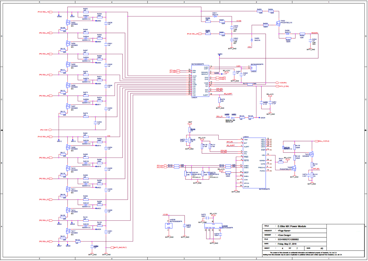
    As you can see, we are implementing a top side MOSFET configuration; this circuit is consuming 100uA to keep enabled the DSG and CHG MOSFET. We decide to implement an integrated charger module (always connected to the VBAT-GND net). This charger is always drawing something around 500uA from the battery pack.

    I performed some lab validation (using a PSU rather than a battery pack) for the following parameters and everything was working ok.

    The Protection\CUV\Threshold is set to 2800mV and the Protection\CUV\Delay is set to 2s.

    The Power\Shutdown\Shutdown voltage is set to 2750mV and the Power\Shutdown\Time is set to 5s.

    OSC160803C02000002.xlsx

    Five systems were tested at customer validation and we detected an issue. When the battery pack State of charge < 40% and stored some months, the discharge related to the charger module keeps discharging the battery pack and reducing the battery voltage. Unfortunately, we observed that CUV protection was not enabled, going directly to the Shutdown mode (the settings file is attached as xlsx file just for demonstration purposes). According to the BQ78350 TRM, the only way to wake up the BQ78350 from the shutdown mode is applying voltage at TS1 pin > VBOOT. This is not allowed to the final user. We are expecting a solution that can be able to use the charger module to wake up the system at any storage time.

    1. Is this the right chipset (BQ78350 and BQ76930) for this application?

    2. If affirmative, What do you recommend to start the debugging process?

    Thanks in advance

  • Hi Tom

    Do you have any news about this issue?

  • The CUV threshold is set to 2800mV and the Shutdown threshold is set to 2750mV, so the CUV should trigger first. Is the device in sleep mode? The voltage is checked every 5s when in Sleep mode, so it could be possible that the voltage dropped through the Shutdown threshold before it was caught. This is not normally the case, because current high enough to do this would normally abort sleep mode and then the voltage is checked at the normal rate. I would try using the resistor divider and slowly reduce the cell voltages to see whether the CUV protection feature triggers.


    You care correct that voltage has to be applied to TS1 to exit shutdown.

  • Hello Thomas

    The CUV threshold is set to 2800mV and the Shutdown threshold is set to 2750mV, so the CUV should trigger first. Is the device in sleep mode? The voltage is checked every 5s when in Sleep mode, so it could be possible that the voltage dropped through the Shutdown threshold before it was caught. This is not normally the case, because current high enough to do this would normally abort sleep mode and then the voltage is checked at the normal rate.

    Yes, at that point the BQ78350 is working at sleep mode. As I mentioned in the last post, the current draw by the system load is around 5uA while current resolution is 1mA; this means that system load current is less than current magnitude necessary to abort sleep mode.

     I would try using the resistor divider and slowly reduce the cell voltages to see whether the CUV protection feature triggers.

    I performed this test at a lab validation using the voltage divider. First, the voltage divider was connected to the circuit at PSU= 31V. Then, the PSU voltage was decreased until reach the CUV protection; once obtained, the DSG mosfet was disabled keeping the CHG mosfet enabled and waiting for the charger voltage. Second, while the CUV protection is activated, the PSU voltage was decreased until shut down voltage was reached; then, the system obtained the shut down voltage status. At this point the validation has an OK status.

    We were making some calculation and even at this extremely low current discharge the shutdown voltage protection must be obtained after weeks or months. My guess is that CUV protection and shut down voltage thresholds are too much close. I am going to make a setup using a battery pack in order to understand the issue. Then, I am going to repeat the test changing the CUV threshold to 2850mV.

    Do you have any other suggestion for the debugging process?

     Thanks a lot for your help Thomas