This thread has been locked.

If you have a related question, please click the "Ask a related question" button in the top right corner. The newly created question will be automatically linked to this question.

UCC28950 Burst Mode Uneven Gate Drive

Other Parts Discussed in Thread: UCC28950

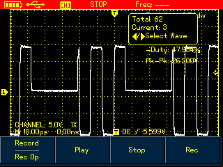
The Datasheet for the UCC28950 shows the outputs A and B, and C and D, having an uneven gate drive (two B pulse, one A pulses) on page 9. This has been confirmed by measurement on my prototype design utilising the UCC28950. One pair is always switching first and that same pair last in the pulse train. Odd switching: volt-second balance != 0

The problem is that it is driving my DC coupled gate drive transformer into saturation during burst mode and causing my gate drivers to overheat. At the moment I have not experienced any issues with my main transformer flux walking, but I probably would do with extended run times.

When I AC couple the GDT, the resultant offset waveform is causing the lower side active leg 'FETs to enter the linear region and they overheat.

Was it designed like this? If so, why?

  • Hello
    The UCC28950 is operating as intended. It is certainly possible to use an AC coupled gate driver transformer with this device and we have successfully done this on the UCC28950 EVM. The schematic is included in the EVM documentation at www.ti.com/.../sluu421a.pdf
    Please have a look at this and re-post if you have any further questions.
    Regards
    Colin
  • I loosely based my design on the application note, and have studied that design.  The problem lies not with the coupling between gate driver and gate drive, but with the controller sending more A&D pulses than B&C ones.

  • Hello

    I ran a quick check on my UCC28950 EVM in Burst mode just now. Some typical screenshots are shown below.

    Yel: Voltage across transformer primary.

    Blu: OUTA

    Grn: OUTC

    I changed the horizontal scale between the two 'scope plots but it is clear that in each burst the power transformer sees an equal number of positive and negative pulses and an equal number of OUTA and OUTC pulses.

    This behaviour is designed into the controller so certainly the OUTx signals at the chip obey this pattern. It is possible of course that something in the gate driver circuit is causing the asymmetry you are seeing. 

    Could you share your schematics with me ?

    If you can't post them here then you could send them to me directly at colingillmorRegards
    Colin

  • As you can see, a very brief pulse is given on MOSFET D at the start of every pulse train. MOSFET C (shown negative) does not have this pulse. This causes the uneven waveform. Exactly the same happens with MOSFET A and B, with A having the erroneous extra pulse, matching up with D's pulse.