This thread has been locked.

If you have a related question, please click the "Ask a related question" button in the top right corner. The newly created question will be automatically linked to this question.

TPS63031 failure?

Other Parts Discussed in Thread: TPS63031

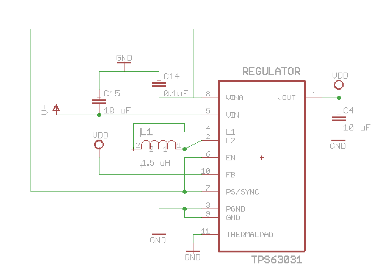
I've been using the TPS63031 for a while (about 180 devices), and have seen a failure that has occurred several times now, and I'm wondering if it's something in my design.

The symptoms are that total current usage rises to > 200mA and the TPS63031 heats up to about 70C, .  The device normally draws around 15mA, and during radio usage, around 30mA.

On a device that has these symptoms, everything is still actually working; the output side of the TPS63031 is producing 3.3 volts as expected, it's just wasting a lot of power and producing a lot of heat.  If I power the 3.3v side of the circuit, I see that it is still drawing a small amount of current (around 12mA). 

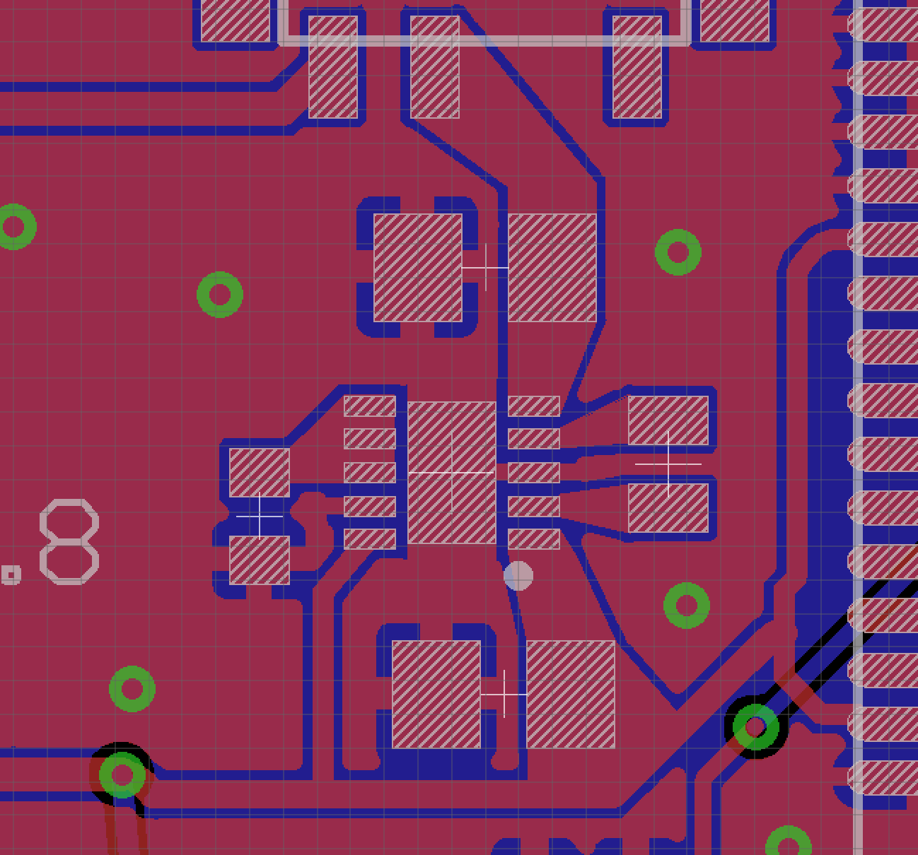
Reading through the datasheet again, I see that I do have the 4.7 μF ceramic input capacitor farther away than recommended; it's about an inch away, near my battery charging circuit.  Could that design error cause the TPS63031 to fail in this manner?

I also notice that I have maybe underspecified the inductor, as its limit is 50mA.

The full design is here.

Appreciate any insight!  Thanks!

  • I am not able to open the design. Can you post your schematic, BOM and layout?
    The layout is a critical part of the design, it can also cause issues, I would like to see the each layer of the layout in PDF with TOP and BOTTOM silk screen
    What is the application behind?
  • Ok, here is the blown up layout: www.evernote.com/.../skitch.png

    The TPS603031 is to the right of center near the top of the board.

    And here is the schematic: www.evernote.com/.../skitch.png

    Seemed like I wasn't hearing issues about this, now I've had a few more boards go bad, so I'm pretty sure it's something systemic.
  • Don't worry about offending me if I've done something stupid. :) I'm not trained in this; just did the best I could based on my understanding.
  • Hi Pete,

    I am running into trouble opening this file. Here is my mail adresss: s-ramalingam@ti.com, can you send them to me directly or use another sharing system?
  • The links worked today. 

    I am not surprised that there were failure, the schematic and the layout  need to be improved.

    Regarding the schematic:

    - I could not find any input capacitor between Vin and Ground, which is mandatory to have. As you can see in the datasheet p11, at least a 4.7 uF input cap is recommended!

    - the output cap seems to be low, a 10 uF output capacitANCE (including the DC bias ) is recommended in the datasheet

    - I would also recommend to add the bypass capacitor between VIA and GND

    Regarding the layout, it is critical to have a good layout to have a reliable and working design for a switching converter. I would recommend you to follow the layout guidelines stated in the datasheet p.15.

    Especially the input and output caps should be placed as close as possible to the device to reduce the parasitic inductance of the trace and improve the capacitance effect.

  • Thanks for the reply.

    Sorry I didn't include enough of the schematic to show the 4.7uF input cap.  It was on the output of the LIPO power manager ic.  I'll attach a full schematic.  It's over by the USB plug in the layout, about 20mm away.

    Also, there are two 10uF capacitors near the output (within 7mm)

    Would the missing bypass cap and the layout differences be enough to explain the component failure?

    Thanks again,

    -Pete

  • The layout is critical to have a reliable design, it could be a strong reason for the component failure. the input capacitor is placed to far away from the device, therefor its effect is totally reduced (and also considering the DC derating), The output capacitor should also be placed as close as possible to de the device . I would strongly recommend a relayout of the design and to follow the datasheet layout guidelines.
    VINA is supplies the internal circuitry, having a capacitor there would help to filter the noise.
  • Thank you for your help.  I have redesigned the board, following the datasheet guidelines, and have made 4 by hand (using a rework station). 

    Unfortunately, on two of the four (after cleaning up soldering issues) started drawing even more current (~ 1A)  when powered up using a bench supply of 4.2V and 1A limit. I reconnected the supply to the 3.3v side of the circuit, and that side was only drawing 18mA. 

    I replaced the inductor just to see, and after replacing it, on both boards, the circuit worked, and drew ~20mA from the lipo side.  So wondering about some issue between the inductor and the regulator, or if I've made a mistake in selecting the inductor. My max current draw is around 30mA. I am using an inductor from digikey: part # 445-1015-1-ND.  

    My layout now matches the datasheet, I have a 10uF cap close to the input, and a 10uF cap on the output, and a 0.1uF cap between VINA and GND.

    Thanks for any insight into what's going on here. 

    -Pete

  • Can you measure the inductor current when the load is 30 mA?
    Which replacement inductor did you use?

    Can you resend you schematic and layout?
  • Sabrina said:
    Can you measure the inductor current when the load is 30 mA?

    I'm not sure how I'd do that. Isn't measuring ac current thru the inductor going to have side effects?

    Sabrina said:

    Which replacement inductor did you use?

    The same inductor; so I assume the one I replaced had failed in some manner.

    Sabrina said:

    Can you resend you schematic and layout?

  • The inductor  is not suitable for this application, the saturation current is too low (50 mA). 

    Even if you have a 30 mA max load Using equation (2) of the datasheet you can estimate the peak current which is beyond  50mA.

    Besisdes in the converter you may have trasient behaviour like at start up (Fig.22 and Fig.23 of the datasheet) where the inrush current is much higher. Therefor the inductor gets damaged and is not acting like an inductor any more

    I would suggest to use an inductor that has a saturation current of at least 1A. I would recommend to take an inductor similar to the one recommended in the datasheet.