This thread has been locked.

If you have a related question, please click the "Ask a related question" button in the top right corner. The newly created question will be automatically linked to this question.

UCD90160 Project File

Other Parts Discussed in Thread: UCD90160, UCD90240

Hi All

I am using the UCD90160 in our board, and I would like to use Fusion GUI to program it

But I don't know how to use the Fusion GUI to program the device

Could you give some step-by-step guide to program UCD90160 with Fusion GUI?

Or is there any example project files for UCD90160?


Thanks

  • Hi James,

    I will suggest you to refer to Chapter 7.3 of UCD90240 datasheet(shown as below). We have a Step by step guide. And the configuration will be very similar to UCD90160.

    ucd90240[1].pdf

    Thanks,

    Luke

  • HI Luke


    Thanks for your reply, I will try it

    I have another question

    We have a third party USB to I2C adpter which can issue I2C write/read to program the device

    and this adpter provides a software to send I2C write/read command

    Could you explain to me how to do the programming with this adpter?

    I want to know what files should be exported from Fusion GUI to be used by this third party software


    Thanks

  • Hi James,

    If you want to code yourself, please go to File-->Export --> Data flash script   to export the script file. 

    I will suggest you to use TI USB dongle and Fusion GUI, it is easy to use and no need to concern about an incorrect coding.

    Thanks,

    Luke

  • Hi Luke,

    Thank you, I will buy a TI USB adapter to try the programming with Fusion GUI

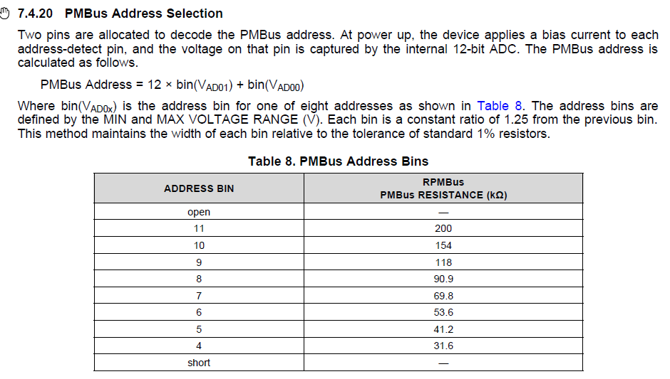
    I am confused with the PMBUS address setting for UCD90160

    The PMBUS addr is set by two analog pins: PMBUS_ADDR0 and PMBUS_ADDR1

    The connection of these two pins in my board is as below, could you tell me what is the PMBUS address with this connection? Thanks


    The related description in datasheet is attached for your reference

  • Hi Luke

    I have another question

    Can the GPO pins be used as SPI bus? I want to use 2 GPO pins to behavior as DIN and SCLK of SPI bus
    Could you tell me how to controll the GPO pins to behavior as SPI bus?

    Thanks
  • Hi James,

    The address will depend on your connection of J37 header.

    For example, if we connect 3-4 and 5-6, it is easy to find the address bin for both pin,that will be 5 and 8.

    So the PMBus address = 12*8+5 = 101

    But if we connect both 5-6 and 7-8 under PMBUS_addr1, the resistor is 43.8Kohm. The address BIN is unknow, it maybe recognized as 5 or 6 randomly.

    We cannot configure a GPIO into SPI interface for UCD90160.

    thanks,

    Luke

  • Hi Luke

    Appreciate for your reply

  • Hi Luke

    In our board, we are using two GPO pins to behavior as SPI bus
    I found there are PMBUS commands to set the state of GPO
    So I want to use these PMBUS commands to drive GPOs to send SPI commands
    This need GPOs can be controlled cycle by cycle

    My questions are:

    Can the GPOs be controlled cycle by cycle with the PMBUS commands?
    Could you give me some guide to controll the GPO pins by PMBUS commands if that is the case?

    Thanks
  • Hi James,

    The GPIOs can be to toggled using PMBus command:  (0xFA) GPIO_SELECT and (0xFB)GPIO_CONFIG.

    Please refer to Chapter 10.43 of below PMBus command reference:

    slvu352c[1].pdf

    You can use TI fusion GUI to help on your coding.

    Go to Tools-->PMBUS Logging ,  press "start logging"

    toggle the pin state of below GPIOs from 1 to 0:

    Then go to Tools-->PMBus Logging, press "Stop logging"

    You should got a spread sheet show as below:

    I hope this will help to complete your coding.

    thanks,

    Luke

  • James,

    SPI clock is usually in MHz. Our PMBus operate at 400kHz clock and it takes tens of clock cycles to send a PMBus command to toggle a GPO. Please make sure that the SPI you are using supports very, very low clock speed.

    thanks,
    Luke
  • Hi Luke

    With your great guide, I can control the SPI interface with GPIO command now
    But I meet a question as below:

    1. I have stored the UCD90160 configuration with STORE_DEFAULT_ALL , and this configuration defines 10 rails and each have a enable
    all voltages out is good
    2. After RESET, I tried to program the UCD90160 again with different configuration, this time I want to just use only one voltage and assigned it a enable. After programmed, NOT issued STORE_DEFAULT_ALL, but other voltages(not defined in Fusion GUI and yet have no enable assigned) which I don't wanted still on.

    With my understanding, the second time programming will override the first time's configuration even I didn't issue STORE_DEFAULT_ALL , so I expect the not defined voltages should be off
    Could you point me some potential causes which lead this issue?

    Thanks
  • Hi Luke

    Some commands used in the second time programming was listed as below:
    This script defined only one rail which with GPIO14 as its enable pin
    I think the SEQ_CONFIG commands will disable all other rails, but they are still on

    // Write SEQ_CONFIG [MFR 38,Rail #1] Rail On Dep: <None> | GPI On Dep: <None> | Rail Off Dep: <None> | GPI Off Dep: <None> | Fault Dep: <None> | Enable: Pin 14 GPIO4 ActiveHigh ActivelyDrivenOutput; Seq On Timeout: 0 / Wait Indefinitely; Seq Off Timeout: 0 / Wait Indefinitely
    I2CWrite 0xCA 0x00 0x00
    I2CWrite 0xCA 0xF6 0x0C 0xAE 0x00 0x00 0x00 0x00 0x00 0x00 0x00 0x00 0x00 0x00 0x00
    // Write SEQ_CONFIG [MFR 38,Rail #2] Rail On Dep: <None> | GPI On Dep: <None> | Rail Off Dep: <None> | GPI Off Dep: <None> | Fault Dep: <None> | Enable: Unassigned; Seq On Timeout: 0 / Wait Indefinitely; Seq Off Timeout: 0 / Wait Indefinitely
    I2CWrite 0xCA 0x00 0x01
    I2CWrite 0xCA 0xF6 0x0C 0x00 0x00 0x00 0x00 0x00 0x00 0x00 0x00 0x00 0x00 0x00 0x00
    // Write SEQ_CONFIG [MFR 38,Rail #3] Rail On Dep: <None> | GPI On Dep: <None> | Rail Off Dep: <None> | GPI Off Dep: <None> | Fault Dep: <None> | Enable: Unassigned; Seq On Timeout: 0 / Wait Indefinitely; Seq Off Timeout: 0 / Wait Indefinitely
    I2CWrite 0xCA 0x00 0x02
    I2CWrite 0xCA 0xF6 0x0C 0x00 0x00 0x00 0x00 0x00 0x00 0x00 0x00 0x00 0x00 0x00 0x00
    // Write SEQ_CONFIG [MFR 38,Rail #4] Rail On Dep: <None> | GPI On Dep: <None> | Rail Off Dep: <None> | GPI Off Dep: <None> | Fault Dep: <None> | Enable: Unassigned; Seq On Timeout: 0 / Wait Indefinitely; Seq Off Timeout: 0 / Wait Indefinitely
    I2CWrite 0xCA 0x00 0x03
    I2CWrite 0xCA 0xF6 0x0C 0x00 0x00 0x00 0x00 0x00 0x00 0x00 0x00 0x00 0x00 0x00 0x00
    // Write SEQ_CONFIG [MFR 38,Rail #5] Rail On Dep: <None> | GPI On Dep: <None> | Rail Off Dep: <None> | GPI Off Dep: <None> | Fault Dep: <None> | Enable: Unassigned; Seq On Timeout: 0 / Wait Indefinitely; Seq Off Timeout: 0 / Wait Indefinitely
    I2CWrite 0xCA 0x00 0x04
    I2CWrite 0xCA 0xF6 0x0C 0x00 0x00 0x00 0x00 0x00 0x00 0x00 0x00 0x00 0x00 0x00 0x00
    // Write SEQ_CONFIG [MFR 38,Rail #6] Rail On Dep: <None> | GPI On Dep: <None> | Rail Off Dep: <None> | GPI Off Dep: <None> | Fault Dep: <None> | Enable: Unassigned; Seq On Timeout: 0 / Wait Indefinitely; Seq Off Timeout: 0 / Wait Indefinitely
    I2CWrite 0xCA 0x00 0x05
    I2CWrite 0xCA 0xF6 0x0C 0x00 0x00 0x00 0x00 0x00 0x00 0x00 0x00 0x00 0x00 0x00 0x00
    // Write SEQ_CONFIG [MFR 38,Rail #7] Rail On Dep: <None> | GPI On Dep: <None> | Rail Off Dep: <None> | GPI Off Dep: <None> | Fault Dep: <None> | Enable: Unassigned; Seq On Timeout: 0 / Wait Indefinitely; Seq Off Timeout: 0 / Wait Indefinitely
    I2CWrite 0xCA 0x00 0x06
    I2CWrite 0xCA 0xF6 0x0C 0x00 0x00 0x00 0x00 0x00 0x00 0x00 0x00 0x00 0x00 0x00 0x00
    // Write SEQ_CONFIG [MFR 38,Rail #8] Rail On Dep: <None> | GPI On Dep: <None> | Rail Off Dep: <None> | GPI Off Dep: <None> | Fault Dep: <None> | Enable: Unassigned; Seq On Timeout: 0 / Wait Indefinitely; Seq Off Timeout: 0 / Wait Indefinitely
    I2CWrite 0xCA 0x00 0x07
    I2CWrite 0xCA 0xF6 0x0C 0x00 0x00 0x00 0x00 0x00 0x00 0x00 0x00 0x00 0x00 0x00 0x00
    // Write SEQ_CONFIG [MFR 38,Rail #9] Rail On Dep: <None> | GPI On Dep: <None> | Rail Off Dep: <None> | GPI Off Dep: <None> | Fault Dep: <None> | Enable: Unassigned; Seq On Timeout: 0 / Wait Indefinitely; Seq Off Timeout: 0 / Wait Indefinitely
    I2CWrite 0xCA 0x00 0x08
    I2CWrite 0xCA 0xF6 0x0C 0x00 0x00 0x00 0x00 0x00 0x00 0x00 0x00 0x00 0x00 0x00 0x00
    // Write SEQ_CONFIG [MFR 38,Rail #10] Rail On Dep: <None> | GPI On Dep: <None> | Rail Off Dep: <None> | GPI Off Dep: <None> | Fault Dep: <None> | Enable: Unassigned; Seq On Timeout: 0 / Wait Indefinitely; Seq Off Timeout: 0 / Wait Indefinitely
    I2CWrite 0xCA 0x00 0x09
    I2CWrite 0xCA 0xF6 0x0C 0x00 0x00 0x00 0x00 0x00 0x00 0x00 0x00 0x00 0x00 0x00 0x00
    // Write SEQ_CONFIG [MFR 38,Rail #11] Rail On Dep: <None> | GPI On Dep: <None> | Rail Off Dep: <None> | GPI Off Dep: <None> | Fault Dep: <None> | Enable: Unassigned; Seq On Timeout: 0 / Wait Indefinitely; Seq Off Timeout: 0 / Wait Indefinitely
    I2CWrite 0xCA 0x00 0x0A
    I2CWrite 0xCA 0xF6 0x0C 0x00 0x00 0x00 0x00 0x00 0x00 0x00 0x00 0x00 0x00 0x00 0x00
    // Write SEQ_CONFIG [MFR 38,Rail #12] Rail On Dep: <None> | GPI On Dep: <None> | Rail Off Dep: <None> | GPI Off Dep: <None> | Fault Dep: <None> | Enable: Unassigned; Seq On Timeout: 0 / Wait Indefinitely; Seq Off Timeout: 0 / Wait Indefinitely
    I2CWrite 0xCA 0x00 0x0B
    I2CWrite 0xCA 0xF6 0x0C 0x00 0x00 0x00 0x00 0x00 0x00 0x00 0x00 0x00 0x00 0x00 0x00
    // Write SEQ_CONFIG [MFR 38,Rail #13] Rail On Dep: <None> | GPI On Dep: <None> | Rail Off Dep: <None> | GPI Off Dep: <None> | Fault Dep: <None> | Enable: Unassigned; Seq On Timeout: 0 / Wait Indefinitely; Seq Off Timeout: 0 / Wait Indefinitely
    I2CWrite 0xCA 0x00 0x0C
    I2CWrite 0xCA 0xF6 0x0C 0x00 0x00 0x00 0x00 0x00 0x00 0x00 0x00 0x00 0x00 0x00 0x00
    // Write SEQ_CONFIG [MFR 38,Rail #14] Rail On Dep: <None> | GPI On Dep: <None> | Rail Off Dep: <None> | GPI Off Dep: <None> | Fault Dep: <None> | Enable: Unassigned; Seq On Timeout: 0 / Wait Indefinitely; Seq Off Timeout: 0 / Wait Indefinitely
    I2CWrite 0xCA 0x00 0x0D
    I2CWrite 0xCA 0xF6 0x0C 0x00 0x00 0x00 0x00 0x00 0x00 0x00 0x00 0x00 0x00 0x00 0x00
    // Write SEQ_CONFIG [MFR 38,Rail #15] Rail On Dep: <None> | GPI On Dep: <None> | Rail Off Dep: <None> | GPI Off Dep: <None> | Fault Dep: <None> | Enable: Unassigned; Seq On Timeout: 0 / Wait Indefinitely; Seq Off Timeout: 0 / Wait Indefinitely
    I2CWrite 0xCA 0x00 0x0E
    I2CWrite 0xCA 0xF6 0x0C 0x00 0x00 0x00 0x00 0x00 0x00 0x00 0x00 0x00 0x00 0x00 0x00
    // Write SEQ_CONFIG [MFR 38,Rail #16] Rail On Dep: <None> | GPI On Dep: <None> | Rail Off Dep: <None> | GPI Off Dep: <None> | Fault Dep: <None> | Enable: Unassigned; Seq On Timeout: 0 / Wait Indefinitely; Seq Off Timeout: 0 / Wait Indefinitely
    I2CWrite 0xCA 0x00 0x0F
    I2CWrite 0xCA 0xF6 0x0C 0x00 0x00 0x00 0x00 0x00 0x00 0x00 0x00 0x00 0x00 0x00 0x00
  • Hi James,

    Your test result is correct. After modifying the configuration, you must  firstly STORE_DEFAULT_ALL, and then RESET the device to see the change.

    Thanks,

    Luke

  • Hi Luke

    Do you mean the STORE_DEFAULT_ALL seems like a configuration loading trigger of the sequencer?

    Without this command, the configuration is not valid or the device will not accept the configuration changes?

    Thanks

  • Hi James,

    STORE_DEFAULT_ALL command is used to store your code from RAM to FLASH.  After STORE_FEFAULT_ALL, please RESET your device, then the UCD90xx will execute your new code in FLASH.

    Thanks,

    Luke