This thread has been locked.

If you have a related question, please click the "Ask a related question" button in the top right corner. The newly created question will be automatically linked to this question.

TPS22920 Manufacturing Question

Other Parts Discussed in Thread: TPS22924, TPS22920

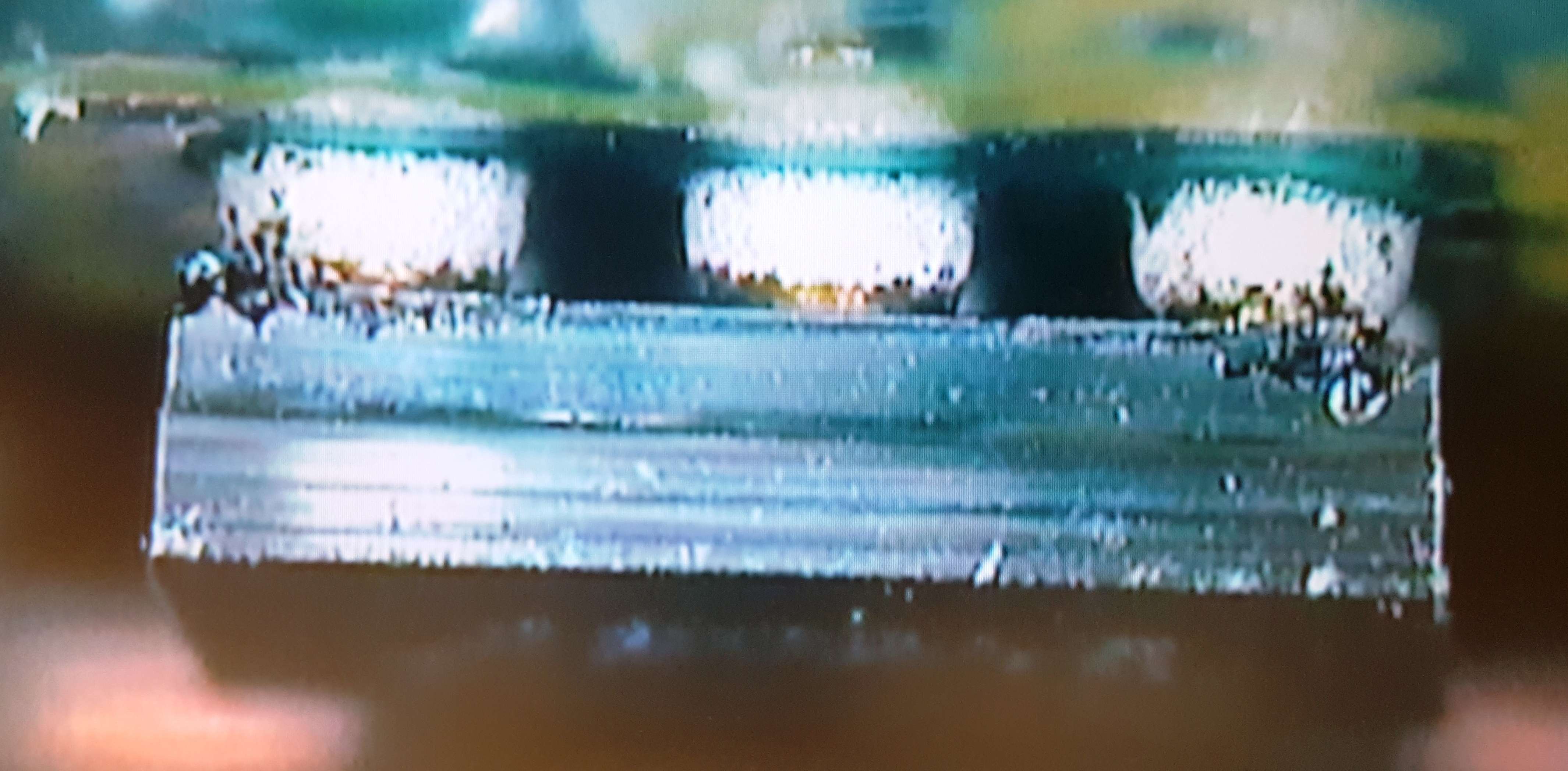
Hello. I'm inquiring about a Load switch. TPS22924 and TPS22920. I work for an electronic contract manufacturing company. I recently assembled a PCB using these SMT DSBGAs using a ROHS process. The customer of this board came back to us claiming that the boards were failing precisely where these components were installed. As I started to investigate our process I noticed that the bodies of these components were damaged. They had crack as if something burst from inside out. The reflow oven profile used to run these boards was tailored for these boards with a peak temperature of 235C. The Datasheet indicates a Peak solder temperature of 260C. These are MSL 1 so moisture wouldn't play an issue. I have pictures of the damage that I would like to share. I'm very inclined to pointing the damage to the design. Can a current or voltage spike break the component body? I would really appreciate your expert feedback. Thank you.

  • Hi Juan,

    Looking at the picture, this looks like die chipping on the corners of the device.  My initial thought would be that the SMT process is causing mechanical damage, but it is hard to tell from the picture alone.  If it helps, we have collateral for SMT processes at Ti.com>Quality>Packaging>SMT & Packaging Application notes.

    To help narrow down the issue, I have a few questions.

    1. Are there any other pictures of the device (from the top or bottom)?

    2. Is this damage seen immediately after reflow, or is it only checked after testing? 

    3. While electrical stress can cause this type of damage, it is dependent on the stress applied.  Does the test program ever bias the device with conditions outside of the datasheet limits?

    Thanks,

    Alek Kaknevicius

  • Hi Alek,

    Thank you for responding to my concern.
    My initial assumption on the damage was the reflow process as well. I've seen this particular damage with moisture entrapment inside components. Can this be the case even though this part falls under the MSL 1 type?

    Unfortunately I'm not certain at which stage the damage occurred. Our quality inspectors did not notice any defects during the manufacturing process. I reflowed a bare board with only this component mounted to try to replicate the problem but no damage appeared.

    My practice is always to review component data sheets for recommended profiling and this was the case for this particular part. . I used a soak profile with a peak temp of 235C using Nitrogen.

    The feedback we got from our customer was that only 2 Locations out of the 5 in which these components are used were failing. Sure enough when we scrutinized the boards we noticed the damage at only these 2 locations. This is why I was inclined to pointing electrical stress as the cause of the problem. If 5 locations use this part, why only 2 show damage?

    I still however need to rule out the SMT process as a cause. The picture I have posted is the one that best shows the damage. The component is so small that is hard to clearly focus even with an ersascope. There was no damage on the top of the component.

    I reviewed the link you've provided in regards to the packaging and smt. I didn't see any points where I would be out of the recommendations.
  • Hi Juan,

    I have reached out to our quality engineer and will let you know their response.

    In the meantime, is there any part of the test which stresses the device beyond the datasheet limits?

    Thanks,

    Alek Kaknevicius

  •  Hi Juan,

    Do you know what the placement force used for these devices is?  I could relay this back to our packaging team to see whether or not this would cause damage to the device.

    Another thought is that the damage is focused at the corners of the device.  This damage can be caused by the package hitting something during placement process, (especially an adjacent component) or by the pick and place feeder when the package is picked up from the tape and reel.

    Thanks,

    Alek Kaknevicius