


Recently, I am designing a Power Bank.
From the datasheet, I learn this chip (BQ24195) works as the following process after the power plug in:
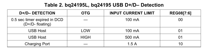
1. The D+/ D- detect whether the power is from the USB or not (from an adapter).
2. Detect the voltage on OTG.
Thus, there are following combinations:
PORT OTG I(limit) BOOST (determined by OTG and Register)
1. USB LOW 100ma CAN'T be used
2. USB HIGH 500ma CAN be used
3. Adapter(>=5v) LOW User's config CAN'T be used
I can understand that, the OTG will be low when adapter is plugged in, because the voltage >= 5v, thus the Q3 in the schematic will must be opened.
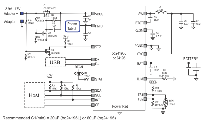
Yet my question is, normally, the usb port is also 5V, thus, the Q3 will also be on, after USB Port is connected, which means that's the case 1. Then the input current is limited to 100ma.
I mean how to use USB port to charge the battery, or a power bank?
Another problem of my circuit is that the current is only 0.09A after I connect the circuit:
From the circuit I summarize the cases that will lead the input current to be limited to 100ma:
1. 0.5 sec timer expired in DCD (This must after the primary detection, I think. I mean this condition will not happen if the chip already know that the power supply is an adapter but not a USB port.)
2. USB HOST and OTG low (HIZ)
3. System rail below 2.2V (Dose this system rail refer to Vsys on SYS pin ?)
4. HIZ
I power my circuit by a DC Power Supply, So, from my analysis, it shouldn't be case 1 and case 2. The Vsys on SYS pin is 3.62 V, so it shouldn't be case 3. Only left case 4. Why the current is only 0.09A? Does it enter HIZ? WHY?


