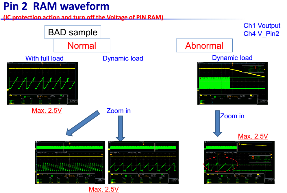
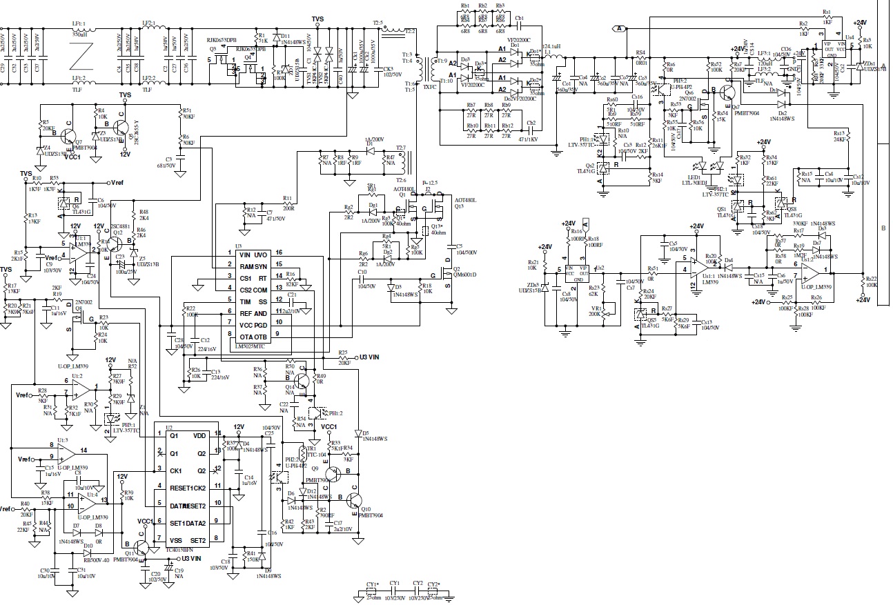
This thread has been locked.

If you have a related question, please click the "Ask a related question" button in the top right corner. The newly created question will be automatically linked to this question.

About LM5025 RAMP Pin Abnormal Phenomenon

Other Parts Discussed in Thread: LM5025

Hi Sir,

My customer currently use LM5025, test dynamic transient load, but have some issue.

Input range 10V~14V, Dynamic transient load(0~4.5A; 50mS ON/ OFF),
occur fail abnormal (@ input 10V), IC occur latch up and no output.

If ok, please let me know which part can effect RAMP pin occur fail abnormal, thanks.
Currently decreas dead time, can reduce RAMP fail, why?

  • Kuo

    Can you post the schematic (with values) and give more details?

    The only latching protection is input UVLO, at minimum 10 V input, maybe this is being triggered? The overcurrent protection via CS2 could also be triggered at minimum input if the current is too big, but this activates a soft restart cycle, it is not latching.


    If you give more information and explain the problem clearly, we can try to help.


    Thanks,
    Bernard
  • Hi Sir,

    update schematic.
  • Kuo

    Unfortunately, I cannot quite understand your question, or understand what is actually going wrong. The resolution of the scope ploys makes them hard to read, I can't see the detailed amplitude of time settings. I also can't figure which plots are good or bad, and what exactly is going wrong.

    Since CS1 is tied to GND, the only over-current protection is via CS2. This will cause a shutdown and soft restart if CS2 level > 0.25 V. However, since the CT ratio is not shown, we can't tell where the trip level will be in amps.

    The RAMP RC components will set a max on-time of ~10 us, with Fsw ~75 kHz, this sets Dmax ~76%. Again, sicne we can't see the main transformer turns ratio, it's to comment if this duty cycle limit is ok.

    The LM5025 has no latching faults, as long the UVLO pin > 2.5 V (plus hysteresis), and if VCC > ~6.4 V. You should verify the VCC level during the testing.

    If the main input voltage (TVS net) is as low as 10 V, the linear reg Q12 may struggle to keep VCC level high enough. there will be a drop across R48/R46 due to the base current of Q12, as well as Q12 Vbe drop.


    Thanks,
    Bernard
  • Hi Sir,

    Currently remove TVS net, and measurement Vcc waveform.

    CT ratio mean transformer turns ratio?

  • Hi Sir,

    if OK, Can you provide your mail address? I can send complete measurement LM5025 waveform for you review, thanks.
  • You can email me at bernardkeogh@ti.com

    Thanks,
    Bernard
  •  

    Hi Nowal,

    If it is a real latch-up instead of hiccup, I would recommend to look into the noise and negative spike coupled onto the IC pin especially Ref and CS. Increasing gate driving resistor of N-FET can reduce the magnitude of the noise. If it works, you can track the path that the noise coupled to the controller especially CS2, VCC and Ref pin. Connecting CS2 to a nearby ground and add a decoupling cap right between supply pin and GND pin of the part can exclude the noise possibility.


    Best Regards
    Frank