This thread has been locked.

If you have a related question, please click the "Ask a related question" button in the top right corner. The newly created question will be automatically linked to this question.

TPS7A4700RGWR – Output voltage at the shutdown

Guru 21045 points

Hi Team,


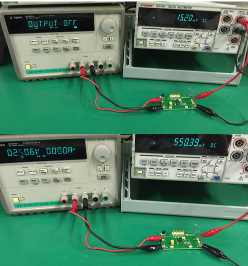
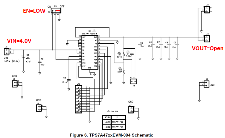
We are evaluating TPS7A4700EVM.

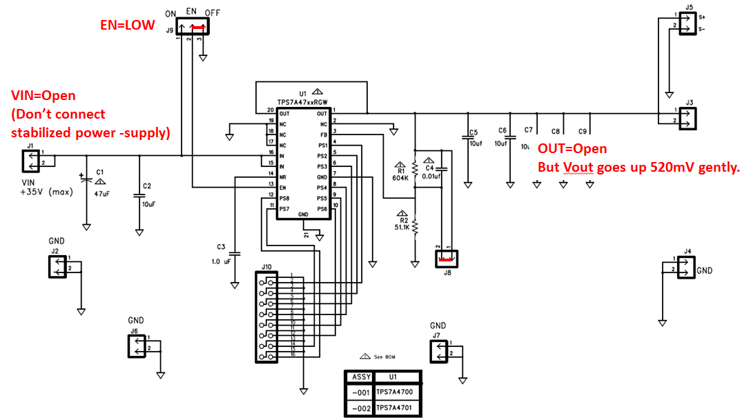
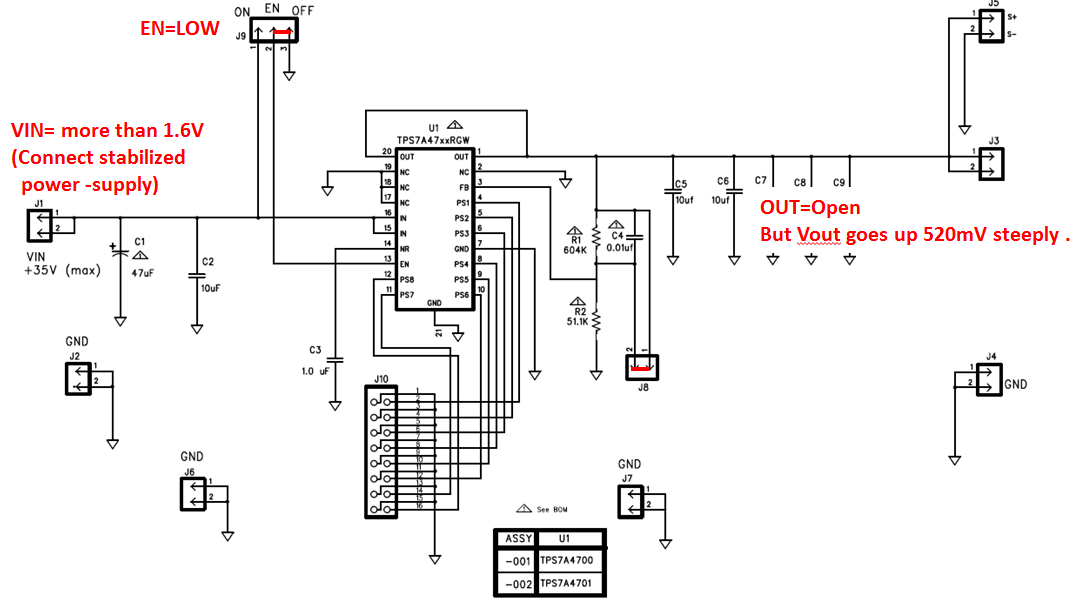
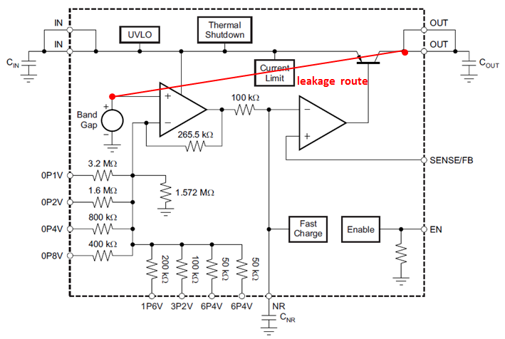
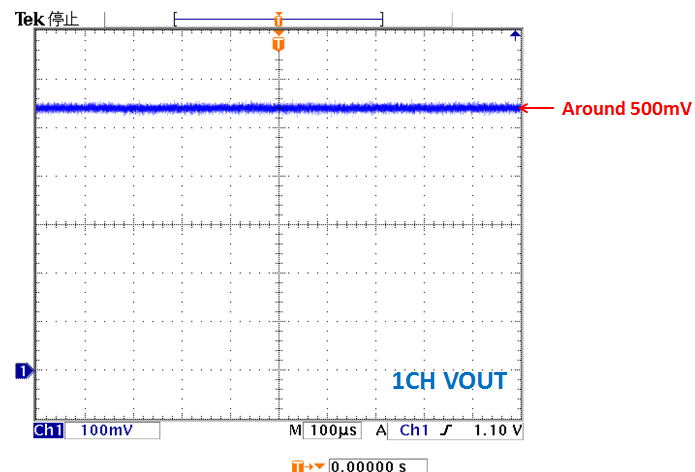
Then, output voltage is around 500mV at the shutdown (EN=Low).

(Please refer to the following waveform.)

Is this behavior right?

If yes, could you please let us know this cause and if you have any workaround?


Regards,

Kanemaru

  • Hi Kanemaru,

    This is not expected behavior. Did you make any modifications to the EVM? Do you see this with multiple EVMs?

    Very Respectfully,
    Ryan
  • Hi Ryan-san,


    Thank you for your prompt reply.

    I didn’t make any modifications to the EVM.

    And I confirmed this phenomenon with one EVM.

    However, this phenomenon is confirmed on our customer’s board.

    So, we guess that this phenomenon depends on TPS7A4700.


    If you contact to below my e-mail address or let me know your e-mail address,

    I can send the customer information.


    [my e-mail address]

    Kanemaru-h@clv.macnica.co.jp


    We do need to explain the cause of this issue to the customer ASAP.

    I’d greatly appreciate your verification.


    Regards,

    Kanemaru

  • Hi Ryan-san,


    I evaluated TPS7A4700EVM-094 (PWR094 REV.A).


    ----------

    [Evaluation content 1]

    I shorted OUT and GND pin when VOUT is 520mV (EN=Low).

    After that time, VOUT returned from 0mV to 520mV.

    -----


    [Evaluation content 2]

    The output voltage(VOUT) rises gently when input voltage(VIN) is not applied (EN=Low).

    And, VOUT rise Steeply if VIN is applied.

    VOUT goes us to 520mV(upper limit).

    Is this behavior right?

    If no, could you please let us know your evaluation method?


    ----------


    Could you please let us know this cause and if you have any workaround?

    I would be grateful if you could reply as soon as possible.


    Regards,

    Kanemaru

  • Hi Kanemaru-san,

    It is interesting that you are reading 520mV even when no power supply is connected to the EVM.  The LDO is not capable of producing an output without an input so there must be a leakage path external to the EVM biasing the output voltage.  From your description, this leakage increases when the power supply is added to the board.

    Very Respectfully,

    Ryan

  • Hi Ryan-san,


    Thank you for your prompt reply.

    I report my measurement environment.

    Could you please let us know if you have any concern?

    And, I hope that you measure TPS7A4700EVM at same conditions.


    I'm thinking about the cause of this phenomenon...

    For example, passes from “Band Gap of internal” to "OUT" exist.

    Then, the output voltage is observed without the input voltage if energy of Band Gap is left.

    May such a phenomenon occur?


    --------

    [Measuring instrument]

    Stabilized power - supply: E3632A(Agilent)

    Digital Multi-meter: AD7451A(ADVANTEST)


    [Result]

    The output voltage in the photograph stops.

    However, this voltage continues gradually rising up to around 550mV(520mV to 560mV).


    --------


    Regards,

    Kanemaru

  • Kanemaru-san,

    From your first schematic drawings I was under the impression that you had jumper J8 shorted.  As a result, I was not seeing the same result as you.  When I opened J8 I measured 200mV.

    This leakage voltage is caused by a small (~300nA) leakage from the supply to the output.  As the pass element is a BJT a small amount of leakage is possible.  When top resistor in the feedback network is shorted, the resistance from OUT to GND decreases and a smaller voltage can be seen on the output.

    Very Respectfully,

    Ryan

  • Hi Ryan-san,


    Thank you for the information.

    Our customer would like to remove the output voltage at shutdown(EN=Low).

    My idea is to connect 1Mohm between OUT and GND.

    Could you please let us know if you have any idea?


    Regards,

    Kanemaru

  • Hi Ryan-san,


    I’m sorry for bothering you again.

    I have three questions.

    And, we do need to explain this to customer ASAP.

    We would be grateful if you could reply as soon as possible.


    ------------------

    [Question1]

    Could you please let us know the upper limit level of the output voltage at shutdown (EN=Low) & Vin=4.2V(max)?

    And, can you guarantee this value?


    [Question2]

    I understand that leakage current is less than 300nA.

    Can you guarantee this value?


    [Question3]

    Is this phenomenon normal operation?

    So, is it the specifications of this device?

    ------------------


    If you contact to below my e-mail address or let me know your e-mail address,

    I can send the customer information.

    I’m looking forward to hearing from you.


    [my e-mail address]

    Kanemaru-h@clv.macnica.co.jp


    Regards,

    Kanemaru

  • Hi Kanemaru-san,

    A small amount of leakage through a BJT while it is off is normal. We do not directly measure this leakage current; however, it is a component of the shutdown current. I(shdn) is equal to the sum of the ground current during shutdown and the leakage current through the pass element.

    The voltage on the output will depend on the amount of resistance to GND. In order to eliminate the voltage, you can implement an external pull-down circuit with a FET and a small value resistor. This will provide a path for the leakage current to ground. The gate of the FET can be tied to the same signal as EN for the LDO.

    Very Respectfully,
    Ryan
  • Hi Ryan-san,


    Thank you always for your kind support and prompt reply.

    I have two more questions.


    ---------------

    [Question1]

    According to your comment, “the leakage current through the pass element”.


    I would like to know the kind of this leakage current.

    So, which of "IS(reverse saturation current)" and " leakage of the parasitic element " is this?

    ---------------


    [Question2]

    According to your comment, “this leakage current is less than 300nA”.


    Does the variability of this current depend on " temperature " and " process "?

    So, we would like to know whether this current becomes higher than 300nA.

    ---------------


    I am very sorry to bother you while you are busy, but I appreciate your cooperation.


    Regards,

    Kanemaru

  • Hi Kanemaru-san,

    The leakage will be through parasitic elements.

    The 300nA current is a typical current. There can be variation at temperature. This leakage will only occur when Vin is high and EN is low. n order to eliminate the voltage, you can implement an external pull-down circuit with a FET and a small value resistor. This will provide a path for the leakage current to ground. The gate of the FET can be tied to the same signal as EN for the LDO.

    Very Respectfully,
    Ryan
  • Hi Ryan-san,

    I’m sorry for the delay in my reply.

    Thank you for the information.

    I will report this information to our customer.

    Regards,

    Kanemaru