This thread has been locked.

If you have a related question, please click the "Ask a related question" button in the top right corner. The newly created question will be automatically linked to this question.

UCC28700: start-up without full energy transfer

Other Parts Discussed in Thread: UCC28700, UCC28730

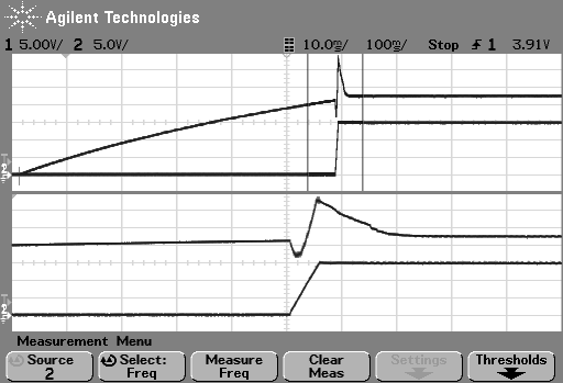
Below, a proper startup-sequence is documented. It was captured while the capacitor on the CS pin was fairly high (1 nF, reference: e2e.ti.com/.../522410).

BTW: a fairly high overshoot in the VDD voltage (top trace, approx. 35V) occurs here. The bottom trace shows a 16V secondary voltage (bulk cap: 220 uF, operating voltage 16V).

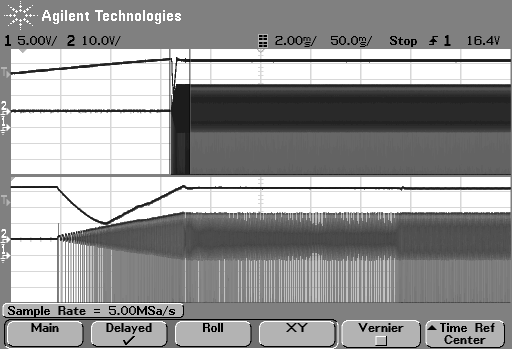
Next capture is without 1 nF on the CS pin (and Vdd capacitor 330 nF) Startup time would be 600 ms without the failed charge in the middle:

After the first Vdd-chargeup, Vdd goes back to undervoltage lockout. The second "try" goes OK. In this case, not the secondary rectified voltage is captured, but instead the voltage on the secondary winding. It can be seen that the switching frequency start quite low, and increases with increasing secondary voltage??

Next, more detail is given. Here, not Vdd is shown, but the voltage on the CS pin (with 100 pF). In the middle, a first PWM start did not transfer enough energy before Vdd touches undervoltage lockout.

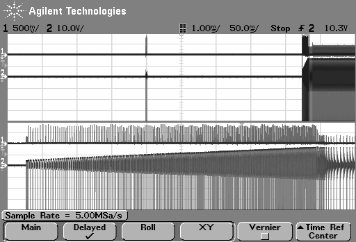
The top trace shows that the CS ramps up to approx. 750 mV (with some variation mainly due to 5MSPS sample rate - zooming has proven that what you see here is truly the top of each current ramp, not any spike). This is Okay. It can clearly be seen that the frequency starts low and then increases. Why is the frequency not at least 44 kHz right from the start? The output capacitor would charge much faster!

Momentarily I'd suggest to increase the Vdd capacitor while also decreasing the resistance of the start-up ladder in order to keep start-up time clearly below one second OR the output bulk capacitor is decreased to 100 uF (which - at 16V would constitute the very same energy as 1000uF @ 16V

But of course it would be better to have 44 kHz right from the start. Any hint about this?

  • Rob,

    There is a lot of info here to analyse. Unfortunately, it would be helpful if we could also see the schematic, with values, turns ratios etc. Would it be possible to post that too?


    From the info above, here are my various comments and observations (not in any particular order):

    - Since the UCC28700 operates in valley-switching mode, it attempts to always switch on a resonant-ring valley, depending on the line/load/output voltage conditions - so the earliest it can switch is on the first valley (in QR mode), or more usually a later valley to hit the target freq set by the modulator (datasheet fig. 15), or sometimes if the load is light and operation is very DCM, it's not possible to valley switch since they have been damped and died away.

    - During startup (or any other time) it's not possible to force a fixed freq, since this could allow the power stage to go into CCM - or more correctly, the DCM-only/valley-switching mode of operation will dictate the freq so as to avoid CCM.

    - During startup, since Vout starts at zero and ramps slowly, the Flyback reset interval will be quite long initially, so the switching freq will be lower as the controller looks for the first valley to start the next cycle. s Vout increases, the Flyback reset interval gets shorter, the first valley occurs sooner, and freq then naturally ramps up.

    - During startup, once Vout has risen sufficiently, the control loop will operate in CC-mode, regulating the Flyback reset interval Dmag duty cycle to Dmagcc (42.5%) while delivering constant maximum Ipk (750 mV). The switching freq will then vary as Vout rises. In CC-mode, a constant average output current is delivered to the output caps/load, so this should give a well-controlled linear ramp up of output cap voltage.

    - Looking at the first plot above, one can see that there is a significant overshoot in VDD as Vout ramps up, yet Vout does not overshoot. This tells us that the primary peak current is large (due to the 1-nF CS pin cap), and also the aux winding leakage inductance is probably large. If the CS pin RC filter is excessive, this will result in higher actual peak current vs the programmed peak current at the CS pin. This will then force the control loop to run at lower freq, since the energy per cycle is higher than it ought to be. The higher peak current will also lead to more energy stored in the leakage inductance, which in turn will cause the Vdd rail to pump up to a higher level - as can be seen in this case. Very often, a small-value resistor is used in series with the aux winding diode (1-10 ohm) to limit the over-charging effect on Vdd due to the aux leakage inductance. Not too, that the RC filter on CS will have a more pronounced effect as input voltage rises - since the di/dt of the current is steeper at higher voltage, the RC delay results in more overshoot.

    - For the second plot, with the smaller filter cap on the CS pin, it looks like the Vdd rail falls too low while Vout is ramping up - there is just not sufficient energy storage in the Vdd cap. The next plot also confirms this. With smaller CS filter cap, peak current is lower (closer to what it ought to be), so the output cap ramp rate is slower, so the Vdd needs to sustain the IC bias power for longer. Moreover, the lower Ipeak means there is less parasitic energy storage in the aux leakage inductance, so again the Vdd rail replenishment from the aux winding takes longer.

    - From the datasheet, eqn 13 estimates the required CVdd size based on Cout and the Iocc charging current into Cout - assuming there is no load at startup. From eqn 13, since the average charging current into the output cap (Iocc) is regulated to a constant, this Iocc value, the size of output cap, and the max load that can be present under startup, are the limiting factors that dictate the required CVdd size - the Fsw does not come into the eqn at all, so increasing the Fsw during startup would not help, except for effects of parasitics (leakage) or non-idealities (peak current overshoot).

    - For your second plot above I assume that there is no output load or very little, since the system succeeds in starting at the second attempt - Vout "staircases" up over a few attempt. If there is enough load to discharge Cout in between startup attempts, then it would not be able to start.

    - If the required CVdd is too large to meet your startup requirement, the startup resistor would need to be reduced to compensate. If the reduced startup resistor leads to higher standby power than can be tolerated, maybe you could consider one the parts in the family with integrated HV startup, e.g. UCC2871x or UCC28730.

    - One other point to note is the amount of required output cap is dictated more by loop stability than by energy storage. As Vout goes up, the required size of Cout for stability may not drop as rapidly and C*V^2 energy storage might imply. If you take a look at the UCC28730 device (more recently released part in the family), there is a an eqn 22 for min Cout required for loop stability - Cout >= (Kco * Iocc ) / (Vo * Fmax), where Iocc is the constant current output limit, Fmax is the max operating frequency at the CV/CC operating corner, and Kco is a constant that depends on the chosen IC in the family. For the UCC28700, Kco is ~400.


    I hope all this info is helpful. As noted above, we can help review the design more thoroughly is that helps, but we would need to see the sch, values, turns ratios etc.


    Thanks,
    Bernard
  • Bernard,

    many thanks for mentioning so many topics in your response. Some of the topics I'll recall now.

    - valley switching: OK, but should have a minor effect on energy transfer per unit of time. More relevant is transformer design, which is suboptimal, as I found out. However: your remark regarding the amplitude of the resonance ringing, which increases with increasing flyback voltage, seems to make sense. However - referring to the second display record - a couple of valleys (with decreasing amplitude) passes by before the switch is activated. I think that the main cause for the linear output capacitor ramp is notified in the datasheet: "The converter remains in discontinuous mode during charging of the output capacitor(s), maintaining a constant output current until the output voltage is in regulation." - as you also say: operating in CC mode and linear ramp.

    The third plot indeed confirms that the startup is not OK yet. Here, below you'll find a trace capture where the output capacitor is 100uF:

    Note: the irregularities in the middle part reflects irregular current consumption due to MCU activity.

    Vdd drops to approx. 10 V. Regarding equation 13 (thanks for attending on this), 100 uF seems a fairly good choice because that equation supposes a voltage drop till 9 V.

    - startup time: thanks for your confirmation that no specific complaint  can be noted about this, expect little more power consumption.

    - loop stability: If you mention that Cout may not drop as rapidly as "C*V^2 energy storage might imply", that isn't true. If you regard that the equation for minimum Cout contains a Iocc in the numerator and Vo in the denominator, and take designed output power as constant, the square relationship holds. My 100 uF selection meets this requirement, after having applied the equation.
    BTW: actually, this is essentially the own drawback of this family of current mode controllers: no capability to trim a compensation network around the error amplifier.

    Thanks for having been helpful to me,

    Rob