Hello,
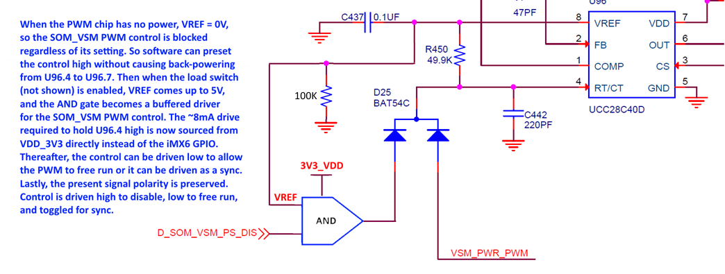
This question is a follow up to my previous thread from a couple of days ago. We have a new need to immediately inhibit the UCC28C40 when its VCC supply is first applied. The least intrusive design change was to add an AND gate as shown in the following graphic:
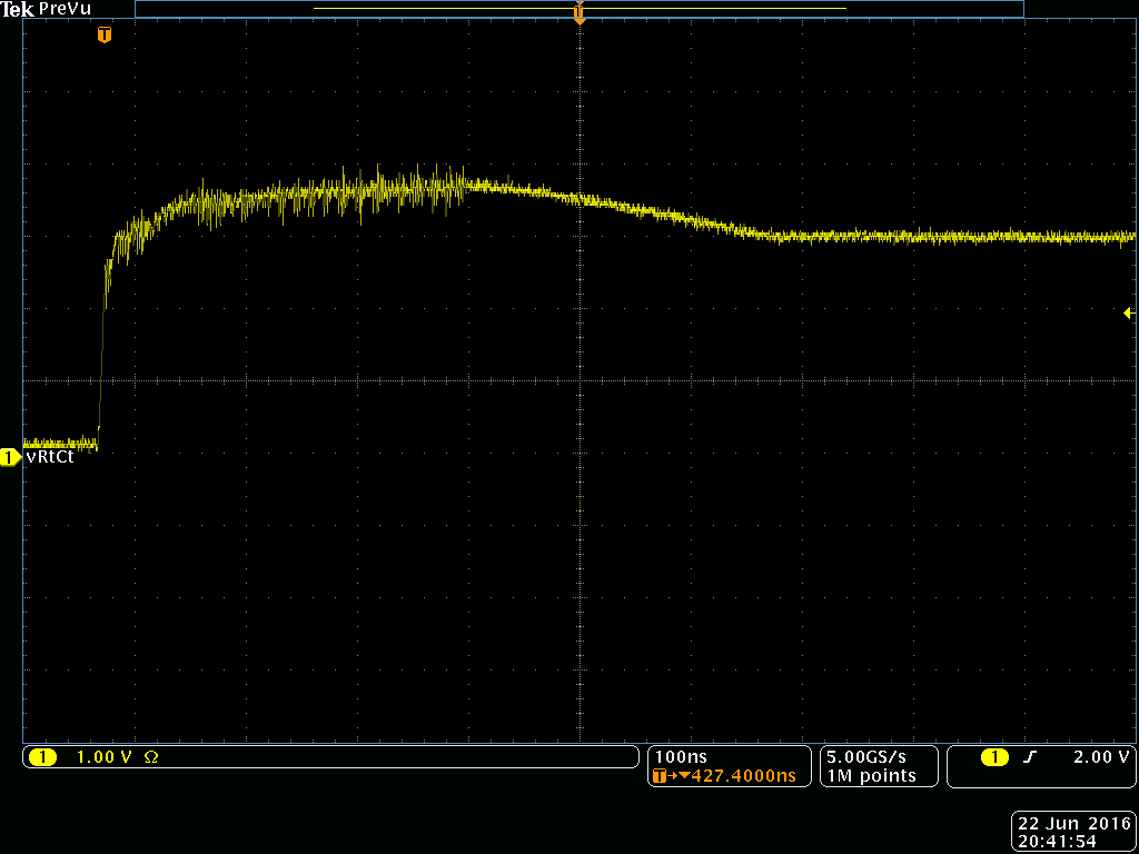
I've tested this and have two concerns. The following scope trace shows where VREF reaches the VIH of the AND gate causing the out drive to the RT/CT pin to go high:
- VREF is only ~1.7V at this point, so technically we are still back-driving the RT/CT pin for another 10us or so. Is this OK?
- I don't know what's causing the leading edge spike. The AND gate is 3.3V output drive and the spike is too long in time duration to be overshoot due to overdrive or common-mode. The voltage is within the maximum specifications for the pin but I'm sure they apply for when VREF = 5V.
I'm having a design review this morning at 11:30am so if it's possible to get some feedback before then that would be great. If not, no worries, I can wait.
Thanks,
Chris
I'm adding a second trace of just the vRtCt transition. This characteristic was captured with a TDP1500 differential probe.


