This thread has been locked.

If you have a related question, please click the "Ask a related question" button in the top right corner. The newly created question will be automatically linked to this question.

LM25118 radiated emission issue

Other Parts Discussed in Thread: LM25118

Hi,

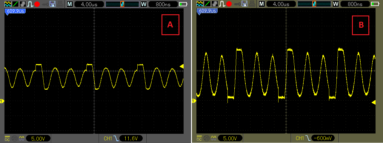
I've successfully implemented a LM25118 buck/boost converter in order to set an output of 16V and drive a load of 200mA. However I'm facing a radiated emission issue around 400MHz as shown

During the layout stage I've followed the datasheet guidelines and this is how it's done currently (top layer).

Seems that everything is okay but I don't know where the problem is.

How can I avoid this radiated interference?


regards,
gaston

  • Gaston,

    Can you send me the design specifications? VIN range, VOUT, IOUT and switching frequency.

    Also if you can probe, both switch node and measure the frequency of any ringing that you see. Capture the waveforms too.

    Are you seeing the radiation emission at the 200mA loading condition?

    -Garrett

  • Hi Garret,

    Thank you for replying.

    Garrett Roecker said:
    Can you send me the design specifications? VIN range, VOUT, IOUT and switching frequency.

    The dc/dc was designed (by WEBENCH tool) for a Vin range of 12V to 24V, Vout=16V and Iout_max=500mA (in my application Iout_max=200mA)

    The switching frequency is set to 300KHz (Rt=18k7)

    Garrett Roecker said:
    Also if you can probe, both switch node and measure the frequency of any ringing that you see. Capture the waveforms too.

    At the moment here's the node A and node B measurements (no load condition)

    Garrett Roecker said:
    Are you seeing the radiation emission at the 200mA loading condition?

    No, the detected emission is at no load condition (Iout=0A)

    regards,
    gaston

  • Gaston,

    Can you zoom in on the waveforms you captured? I've circled the areas I would like you to focus on. There is usually some ringing on switch node in the frequency range you are seeing.It is usually small in amplitude and is caused by parasitic capacitance on the switch node.

    Just to clarify you are only seeing elevated radiated emissions at no load?

    Thanks,

    Garrett 

  • Hi Garrett,

    The observed ringing is about 200MHz. I'm not sure if it's the expected value (f_interf = f_ringing x 2) or it's caused by my oscilloscope limitation (BW = 200MHz). Anyway, how can I mitigate this ringing? Can I implement a snubber network? Where exactly? I think the section 9.2.2.16 in LM25118 datasheet does not clarify this enough.

    Garrett Roecker said:
    Just to clarify you are only seeing elevated radiated emissions at no load?

    I see the same interference with or without load.

    regards,
    gaston

  • Hi Garrett,

    Any hint to implement a snubber network or another workaround for the emission reduction?

    regards,
    gaston

  • Gaston,

    The simplest way to design a snubber is thinking of it as a low pass filter. Select a cut off frequency below the switch node ringing frequency and select the resistor and capacitor that meet that cut off frequency. Capacitors are usually selected to be in the 100's pico-farad range. Then the resistor power rating can be estimated by the below equation. 

    Presistor = Csnub*(Vin^2)*fsw*(1+M)

    Where 

    Presistor = Snubber resistor power rating 

    Csnub = selected snubber resistor

    Vin = Input voltage

    fsw = Switching frequency

    M = Margin (Usually give a minimum of 30%)

    The snubber can be placed on the buck switch (Point A on your drawing above). If the radiated emission issue still exists then another snubber can be added to the boost switch node (Point B on your drawing above).

    This article would be a good starting point to of other techniques to reduce switch ringing. 

    -Garrett

  • That's great Garret! The ringing has decreased as shown with a 680pF and 1R snubber network

    Now I just have to perform EMC tests again

    many thanks,

    gaston