


Hello,
I have a TLC5951 Eval board which I am driving using an FPGA (I removed the DSP module and connected my FPGA signals to J9 to take its place). It seems that my grayscale data is being latched in properly, but for some reason, the DC/BC/FC/UD data is not. I know this because the DC/BC/FC/UD data being returned to me on the GSSOUT output is not what I sent in. In fact, the DC/BC/FC/UD returned to me changes every time I capture it. I suspect the problem lies with the order of events required to dump the DC/BC/FC/UD shift register into the DC/BC/FC/UD latch (where it will take effect). For convenience, I am simultaneously shifting in GS data and DC/BC/FC/UD every display time (30 Hz). The data rates are the same as the DSP provided signals (25 MHz shift clocks). Here's a capture image:
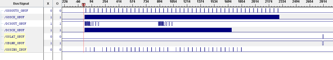
Sorry if that's illegible. The signal order is:
GSSIN
GSSCK
DCSOUT
DCSCK
GSLAT
XBLNK
GSSOUT
Everything is doubled in length because I am using the two devices in series, as it is wired on the board. So I shift in 576 bits of GS info and 432 bits of DC/BC/FC/UD info. The data returned on GSSOUT does not look anything like the data I sent in and seems to change all the time.
Any ideas what I'm doing wrong? If there were a VHDL/Verilog model of the digital portion of the 5951, that would be very useful.
Thanks for any help,
Alex Duque
Alcatel-Lucent
