This thread has been locked.

If you have a related question, please click the "Ask a related question" button in the top right corner. The newly created question will be automatically linked to this question.

LMR62014 and LMR27313 circuit design issues

Other Parts Discussed in Thread: LMR62014, LM27313

Greetings ,

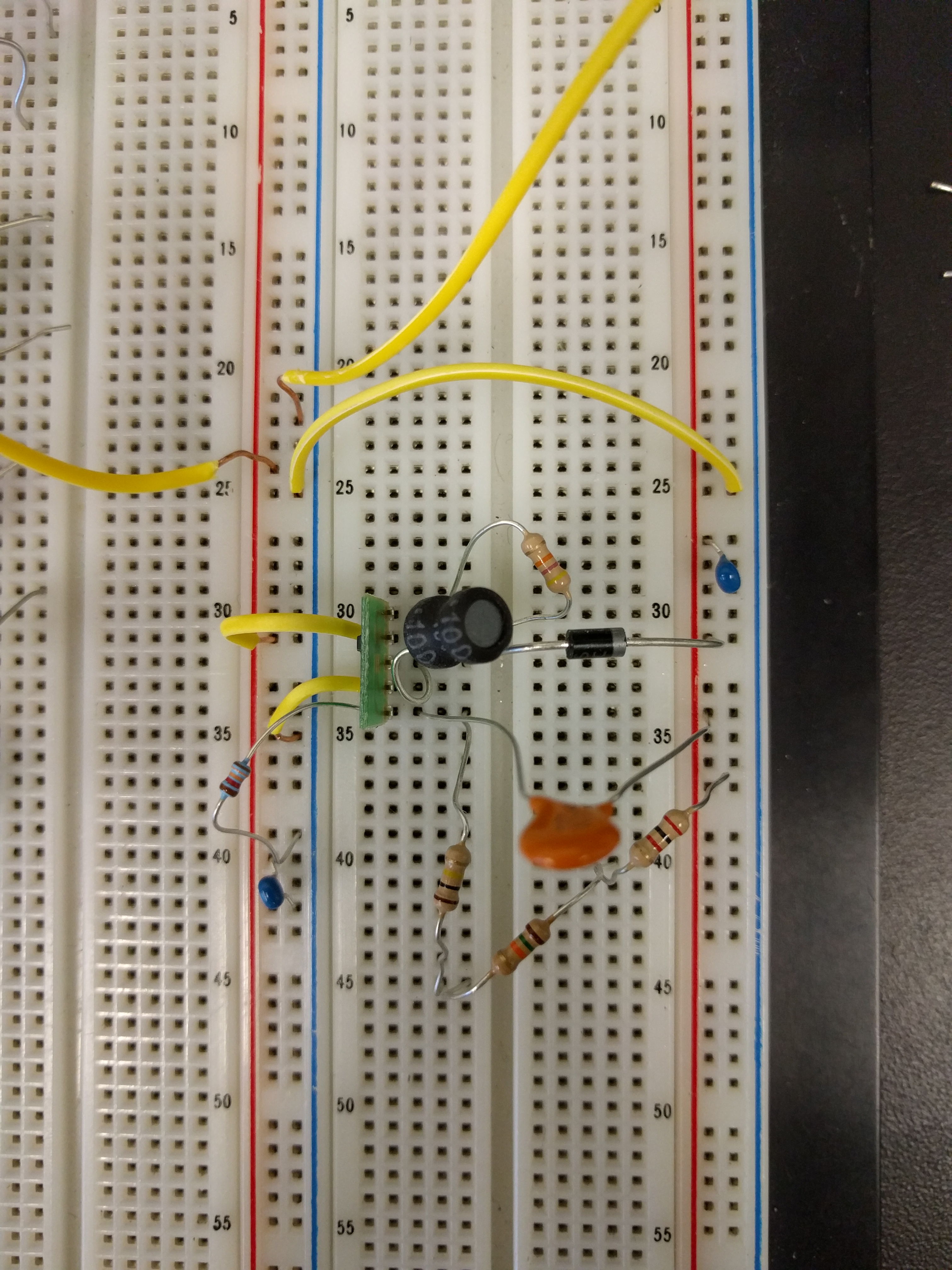
I recently purchased several of both LMR62014 and LMR27313 IC's for a voltage step-up application. I want to step up voltage from 12V to 18V and the circuit it will feed into requires between 50mA and 590mA. I used the online datasheet to help size and design the circuit but have been unsuccessful in producing my desired output. I have also attempted to recreate the example circuits provided at the beginning of each datasheet but got some extreme results. I will outline a few circuits i've tried below:

Try 1: attempt to recreate the example circuits

Vin - 5

R1 - 117K

R2 - 13.3K

R3 - 47K

L1 - 10uH

C1 - 2.35uF (ceramic)

C2 - 4.7uF (tried ceramic, ceramic and electrolytic, and electrolytic)

Cf - 225pF (ceramic)

D1 - SB130-T (30V schottkey diode with a 1A current rating and 500mV leakage)

This produced an output oscillating between 19.3V and 21.5V while the expected is 12V

Try 2: attempt to achieve 18V output from 12V input

Vin - 12

R1 - 180K

R2 - 13.3K

R3 - 47K

L1 - 10uH

C1 - 2.2uF (ceramic)

C2 - 4.7uF (tried ceramic, ceramic and electrolytic, and electrolytic)

Cf - 150pF (ceramic)

D1 - SB130-T (30V schottkey diode with a 1A current rating and 500mV leakage)

This produced between 23V and 26V output which I thought exceeded the output max

Try 3: attempt to adjust R1, R2 to achieve desired output

For this application I stepped the voltage up as I found whether I was producing a good ~18V output however once I got to a 10.5V input the Vout matched Vin. The design kept capacitors C1 and C2 the same as above and Cf changed slightly with respect to R1.  Keep in mind for this try I was not doing precise calculations as I did before, this was more trial and error.

R1/R2/Vout/Vin-turnoff limit:

180k/12k/26V/9V

150k/11k/19V/10.5V

100k/11k/18V/10.75V

100k/10k/18V/11V

This however is an issue because I need to be able to take ~12V in and send ~18V out for my application to work. 

A couple thoughts I had were, do I need to have some load connected for the circuit to function correctly?

Is there a calculation or component that I am missing?

Any ideas as to why I was unable to recreate the example circuits?

  • Hi Michael,
    Are you using the TI EVM, or are you prototyping your board another way?
    While the converter is running does the input voltage look DC or is it oscillating?

    Marc
  • Hi Marc,
    I'm not using the TI EVM, I bought several SOT-23 breakout boards from digikey and double checked the continuity with a multimeter to make sure the solder points were connected well. The power supply I am using is a DC programmable power supply with 3 channels so that I can set everything directly. It has a digital read out of Volts, and current. One thing that happened a few times, I can't quite remember the combination of components, was that the current was oscillating about 30 mA then it sharply rose until it reached the power supplies limit which forces the voltage to drop. Other than that happening the power supply input is completely DC.

    Thanks,
    Michael
  • So the important thing is going to be how cleanly the layout is on the breakout board. You are going to want to make sure that the output cap ground and the ground of the ic are right next to each other, no long wire from one to the other. This is the noisiest part of the circuit, so tends to cause noise issues if not layed out correctly. Basically follow the instructions on page 10 of the datasheet.

    Marc
  • I will try to make sure that the components are closer per page 10 on the data sheet. I was curious though, would lots of excess noise cause the voltage output to always be significantly higher than calculated?

    -Michael
  • It could. I have seen noise on the FB of a different part cause the output voltage to drift up. I am just starting at the basics. Layout can cause a lot of trouble with switching power supplies that you would might get away with on a logic design. So it is often the first thing to look at when the Bill of Materials looks reasonable.
  • I tried it out today with shortening all the leads of the components as much as possible and shortening distances between the LMR62014 and its IO but I didn't see a noticeable change in performance. I'm still getting the 19-23V output from the 5V input while I expect a 12V output. I am going to continue seeing if I can find the culprit to my problem. Do you know if the type of inductor would have any affect on the circuit performance? I would assume a magnetic field could cause some problems. Is there any reason that the voltage divider computation would be incorrect? The one given on the LMR62014 is 

    R1 = R2 X (VOUT/1.23 − 1) 

    While the equation given for the LM27313 is 

    R1 = R2 x ( (VOUT / VFB) − 1 )

    My feeling is that the first equation is simply missing a parenthesis  but I could be wrong.

    Any ideas?

  • Hi Michael,

    Order of operations wise both equations are identical, but you are correct that the second is easier to read.

    What type of inductor are you using?  The shielded inductors, contain more of the magnetic flux than the un-shielded inductors.

    Can you send a picture of your setup?  Maybe I can get a clue from that?

    Marc

  • Marc,

    The inductor I have is a RLB0712 from Bourns Inc. It is an unshielded inductor with a ferrite core. 

    The picture shows my setup, the green pcb is layed out where the IO from top to bottom are: SHDN - Vin - SW - GND - FB

    Also, I didn't have a 117K resistor in stock so the picture shows I am using 100K, 15K, and 2K in series.

    Currently I don't have any load attached to it, is that a requirement to get a desired output?

  • Hi Michael,

    My guess is that you are getting a lot of noise from the boost do to the long wires on the ground leads.  Specifically the ground of the output voltage cap and the wire connecting the part to the ground bus you are using.

    If you send your details to simpleswitcherapps@ti.com i'll see if I can find an eval board for the part that you can look at your design on.

    Regards,

    Marc