This thread has been locked.

If you have a related question, please click the "Ask a related question" button in the top right corner. The newly created question will be automatically linked to this question.

TPS40170 Shootthrough Issue

Hello,

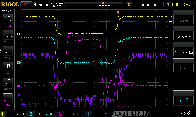
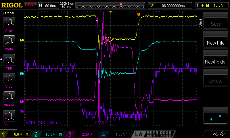
I have  a TPS40107 design that I'm experiencing FET shoot-through on. Here's scope traces of both FET gates:

Blue trace is upper, yellow is lower. Lots of ringing on both gates.

Here's the schematic:

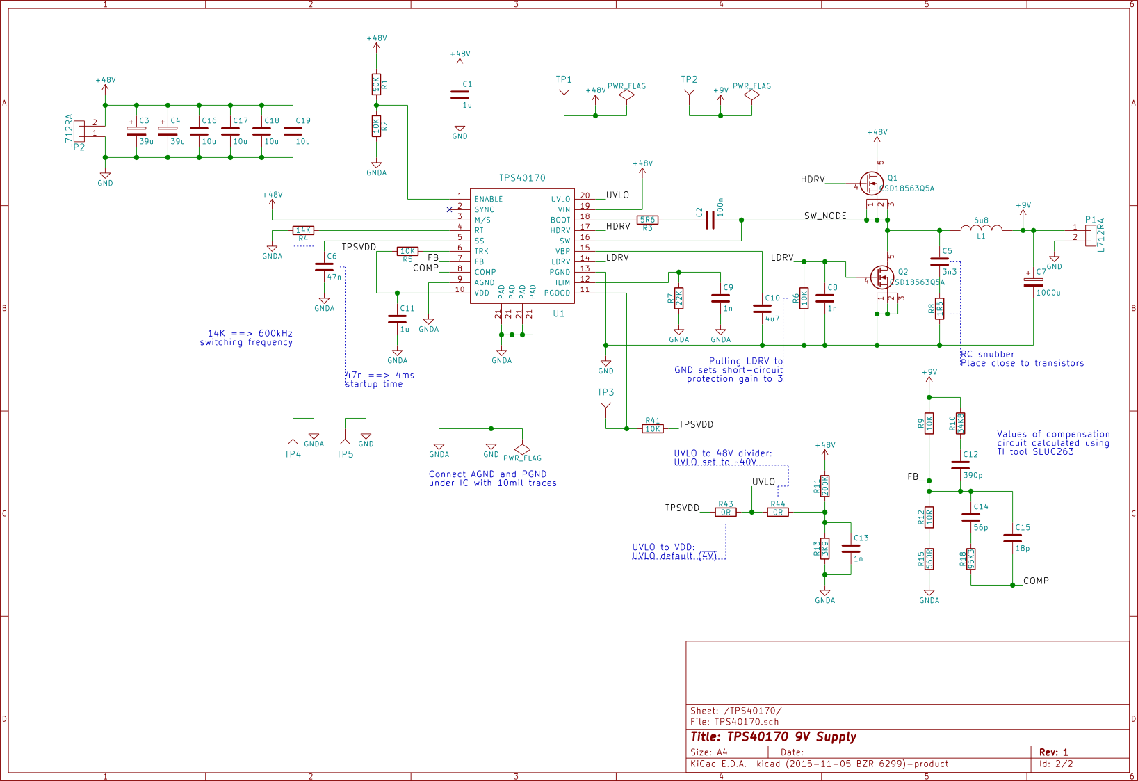
The design is for a 48V input, though I'm currently using 15V to prevent the FETs from burning out.

I've experimenting with changing the value of the RC snubber, but there is no/very little change to the behaviour of the circuit.

Thank you, any help is appreciated.

  • Sorry for bumping this, I'd really like to get some guidance.

    Can anyone suggest anything? Is there more information I can provide?
  • Let me see if I can find someone to help.
  • Hi,

    First, can you take C8 off?
    The blue trace in your waveform is the voltage between HS gate and GND, we need to check Vgs of high-side FET.
    Please measure the Vgs of high-side FET and low-side FET at the same time.
    If you don't have a differential probe to measure high-side Vgs, please use two probes to measure high-sidge gate and SW, then get Vg-Sw=Vgs.

    Thanks
    Qian
  • Sorry for delay in replying, I was diverted onto other projects.

    We don't have a differential probe, so had to use math function on the 'scope. As requested, here's traces for highside and lowside Vgs:

    On both images:

    Channel 1, yellow: Switch node

    Channel 2, blue: Highside gate

    Channel 3, pink: lowside gate

    Math, purple: Ch.2 - Ch.1

    I don't know how to interpret these traces, so hopefully they can provide information that helps you.