This thread has been locked.

If you have a related question, please click the "Ask a related question" button in the top right corner. The newly created question will be automatically linked to this question.

LM5113: HS to VSS undershoot

Other Parts Discussed in Thread: LM5113

Im driving EPC2032's from the LM5113, and more often than i'd like, Im having fet failures.  The project is a motor drive, so essentially its acting as a synchronous buck converter most of the time.  While some failures seemed to be related to soldering (too much heat, or too long) and other failures due to my own accidents, I'm still having failures that I can't track down the real cause.  All of the failures until the most recent one did not damage the gate driver IC.  I give this background, because, I really have low certainty in any of my theories about what's going wrong.  

My board design is essentially a rip-off of the EPC9013 demo board: 

Except im using the EPC2032 instead of the 2001.  Also, my board is 6 layer for increased current handling, and im trying to stack 4 of the boards in parallel to handle higher currents up to 200A.  

So on this last failure, all of the high-side fets were nearly blown off the PCB, while all of the low-side fets measure perfectly fine (and, indeed, work fine now that the bad parts were replaced).  The high-side gate driver shows that there was a failure in the isolation section, as the driver output measures 20 ohms to Vss.  My suspicion is that the gate driver failed first, and killed all the high-side fets by applying -Vsupply (50V) to the gates essentially.  Input voltage to the bridge was 50V, and i have not seen any overshoot in excess of 10V on the output.

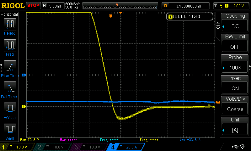
When i look at the HS pin vs VSS i see up to -8V excursions (lasting 5nS or so).  Matching my over-shoot and ringing frequency (~250MHz) to a spice sim suggests i have about 100pH of total power loop inductance.  I don't know that i could do any better.

I tested a new driver to destruction and found that it took -15VDC from HS to VSS to kill it (while there was 5V on VCC to VSS).  The resulting breakdown gave a similar low resistance from the high-side output to Vss as the gate driver that failed under use.

When i probe the EPC9013 demo board i see the same -8V excursion (70VDC input, switching 35A).  I am of course, probing as close to the IC pins as possible and not using the long ground lead on the probe.  The scope capture shows HS-VSS on channel 1 (yellow) and load current on channel 4 (blue).  

So, how serious is this transient?  I figure it can't be too bad, or else EPC probably wouldn't get away with it.  Any insight into how sensitive, or how predictable (or unpredictable) damaging the isolation well is would be useful for me.    

  • Hi Steven,

    Though I can't say I know exactly what your problem is, I can give you more clarification on the effects and failure modes associated with pulling HS below VSS. The isolation on die is achieved by placing the high-side driver in a large n-type tank connected to HB which is sitting in the p-type substrate connected to VSS. So, the real constraint is when HB goes below VSS, this diode turns on and works to charge up the bootstrap capacitor. Though I'm not aware of any specific problems it causes, it would not be surprising to find that turning on this diode could also cause some internal circuits to malfunction because a bunch of the internal circuit nodes now become parasitic collectors of a parasitic PNP and will have current injected into them. However, this PNP has a very low beta, so there may not be any problems.

    When you tested the driver to destruction in DC by pulling HS down below ground, what probably happened is this diode kept HB at a diode drop below ground and the driver failed when HB-HS supply voltage became too large. The HB-HS over voltage driver failure is probably not the failure mechanism you are seeing in the dynamic case though, nonetheless, the FET gates are much more sensitive to overvoltage than the driver is, so FET damage could occur in the dynamic case. The normal HB-HS voltage regulation scheme cannot control the bootstrap voltage and prevent FET gate damage in this case as it only controls the normal bootstrap diode charging path, not the parasitic HB-VSS diode charging path. Therefore, if you haven't already, I'd take a look at the HB-HS voltage during operation to see if it is getting charged too much which could be causing some FET failures.

    In the dynamic case when HB-VSS goes negative, some current will flow through that diode. Though it is a physically large diode, the current path goes through a high-resistance substrate so the current will be somewhat limited. If we assume HB-HS is 4.5V, then the voltage across this diode with HS=-8 is 3.5V. The inductance of the path will also limit the current. I would guess the instantaneous current would be on the order of one amp. Nonetheless, there will be a point where it would fail, but I'm not sure where that is.

    Hopefully this gives you some more information, As mentioned previously, I would check the HB-HS voltage and watch the HB to VSS voltage. Measuring how much current is flowing in this HB-VSS diode in the dynamic switching case would be difficult, but might be possible. One could also characterize the diode on a curve tracer to see what to expect.

    Regards,
    Nathan
  • Hi Nathan,

    Thank you for that.  So if i understand, there is an extra diode from VSS to HB, and the internal regulation of HB to HS cannot control the unintentional charging by this extra diode, and this is the reason (maybe just partly) for the -5V spec on HS.  

    I don't have a differential probe to catch HB-HS properly and my attempt at some common-mode isolation by wrapping the probe through a ferrite core didn't work either.  However, measuring HB to VSS, i can clearly observe the negative voltage spike, but i don't see any indication of significant charging of Cbs, because as HS returns to ground voltage (some 20nS later), HB - VSS never exceeds 5V.  Cbs is 1uF, so even an amp for 5nS is 5nC which is 1000X less than the 5uC in Cbs.    

    I guess there might be something to your first thought, that turning on the VSS-HB diode is upsetting something else.

  • Hi Steven,

    It sounds like the HB-HS voltage is not getting charged up excessively. The parasitic PNP structures in the driver would probably just disrupt the UVLO on the high-side and cause the the part to go into UVLO for a time before coming back out. It should not cause catastrophic driver failure like you are seeing. A more likely candidate would be the transient over-current event through that HB-VSS diode is enough to blow it. 

    Regards,

    Nathan

  • Hi, Steven,

    Did you get this issue resolved? If so, what was the root cause, and how did you resolve it?
  • Hi Don,

    I still haven't found what's going wrong.  At this point I'm trying to stress them in various ways to see why it fails.  Unfortunately, capturing a failure on the scope has been challenging, and so far I have yet to get a clear picture of what initiates the failure.  The last failure, for example, was operating fine at 70V supply for several minutes, but the moment i increased the supply to 75V it let out the magic ;-).  Unfortunately i was left with a scope capture well after the failure initiated, so very hard to make sense of it.  To make sure it's not just voltage sensitivity, i tried another fresh board at 90V and it seems fine.  

    I've been working with a ltspice model, which is quite excellent at matching my measurements except for the magnitude of the under-shoot measured on the output node of the bridge.  The main discrepancy i see with the EPC2032 part in spice is that its effective output charge (Qoss) is larger than the real parts on my board. The measured rate in voltage change during a ZVS switch transition is a good bit faster than what the simulator predicts for a given load current and supply voltage.  

    I note that the ringing frequency of my board is ~250MHz, and yet im using a 100MHz scope (1GS/s, however).  The only time i can even detect ringing on the switching events is during low-voltage, high-current stress, switching 200A @ 30V among the 4 parallel fets.  Spice predicts a far greater ringing amplitude than i record, but the frequency of the spikes is >200MHz, so i suspect i'm simply not getting a clear picture of what's really going on.  New scope is on the way...  I'll update if i figure anything out.

  • Hi, Steven,

    Any luck?

    I just reviewed the thread and noticed that you mentioned you have FETs on four different boards? Have you read EPC's app note on paralleling GaN FETs? Actually, it's in their book on GaN... I found this video on their website, it seems they haven't published this chapter separately.

    epc-co.com/.../ParallelingeGaNFETs.aspx