This thread has been locked.

If you have a related question, please click the "Ask a related question" button in the top right corner. The newly created question will be automatically linked to this question.

bq24600 charger ic thermal pad

Other Parts Discussed in Thread: BQ24600

hey,

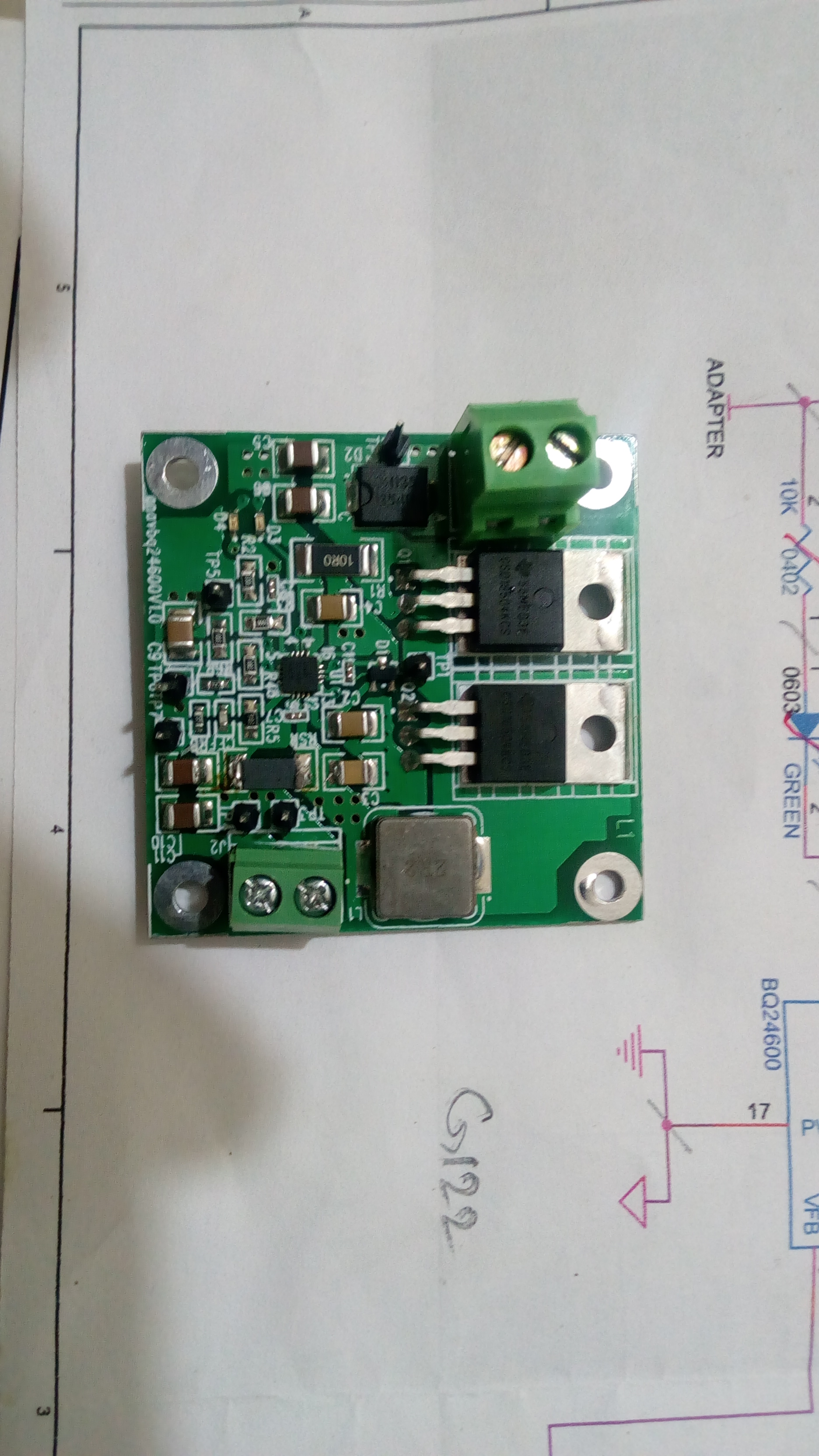
I am designing the 10 A and 4 series cell charger for the li-ion battery pack. I made the circuit as given in the data sheet for bq24600 but the circuit is not working, one thing I find odd in the PCB is that PCB guy does not make the thermal pad connections with the ground. does thermal pad must be connected to the ground for the operation.

Thanks

  • Hi Vijay,

    Use the EVM user guide as a reference. As for the thermal pad, it is not necessarily needed, but it is recommended to connect it to the power ground plane to dissipate heat, especially when you plan to charge 10A 4S battery.

    Regards,
    Steven
  • Hi Steven,

    Thanks for your reply, I design the circuit as given in the datasheet for 3A ,single cell but I use the electrolytic capacitor and make the circuit on breadboard hence the length of wire is 10- 15 cm for each  connection with bq24600 IC , instead of using single 10 milliohm sense resistor I am using 10 resistors of 100 milliohms in parallel to make 10 mil ohms.I know this kind of design is very sketchy I am able to get only 70mA current for the circuit.if I am doing wrong. can you suggest me guidelines to make such kind of charger circuits ?. SMD devises PCB  facility is not available nearby me.

    Thanks

    Vijay Singh

  • Vijay,

    Using a breadboard will be very noisy and not ideal for a charger to work. These chargers require good sensing to make precise calculations. Using long cables and also not using a uniform ground will create problems. I suggest creating a PCB somehow to accurately test this charger.

    Regards,
    Steven
  • Hi Steven, 

    thanks again! 

    I am looking for the PCB development and taking help from datasheet and evm guide and made a list of components which are available in India. some of the components are not available so I make some changes. please, could you check the list and let me know that I am going in the right direction.it will be a great help as I am new to the SMD devices PCB.

    PLEASE FIND THE ATTACHES DOCUMNT.

    Thanks

    Vijay Singh


  • Hi Vijay,

    For the FETs, look for one with less Qg, below 20nC. You don't need to use 10mohm if it is not available, you can use 20mohm, just make sure to take it into account when you calculate ISET. If you follow our EVM guide closely, you will have a good schematic: www.ti.com/.../sluu410.pdf .

    Regards,
    Steven
  • Thanks for your support. i am looking forward for pcb

    regards

    vijay singh
  • Hi Steven,

    I completed the design for schematic and PCB. can you review once and give your comments so i can move further for fabrication.please find the attached  schematic and PCB file.

    ThaSchematics_Charger board_210716 (1).pdfCharger Board_240716.pcbnks

    Vijay Singh

  • Vijay,

    Good to see you were able to make a pcb layout. Can you send me a .brd file so I can open in Allegro? What program was used to produce pcb file?

    Regards,
    Steven
  • Hi Steven,

    Mentor Graphics software is used to make the design. The .pcb file can be opened using Mentor graphics pads pcb viewer, which is free available at website. Here is the link  https://www.pads.com/downloads/pads-pcb-viewer/.  also i attach the gerber files.

    Please comment on design, so i can take next step of fabrication.

    Thanks for your support.

    Vijay Singh

    anavbq24600V1.0.zip

  • Vijay,

    You may need to add more copper pour for GND so that heat can be dissipated. Other than that, the layout looks good. I would place C8 and C9 closer to the Q1 drain.

    Regards,
    Steven
  • Hi Steven,

    Thanks for your comment at present i am making circuit up to 5A so so can go with this design ? in the next design i am looking for 10 A charger so i keep in mind your advice to add more copper pour and placing of capacitors. could you please tell me a knowledge source regarding circuit and pcb design so i know how to make great design for chargers.

    Thanks

    vijay singh
  • Hi Vijay,

    Of course, you can look at these app notes to get a feeling on how to optimize the layout for buck converters:
    www.ti.com/.../slyt614.pdf , this has FETs integrated, but the same concept. Just think of the IC pins as the FET drain and source. Explains the importance of keeping signal traces away from the power path. Use separate analog and power ground with a single point connection.
    www.ti.com/.../slyt465.pdf , this helps with ringing on the switch node, giving you four alternatives to reduce it
    www.ti.com/.../slpa010.pdf , this one also talks about ringing, and includes an example optimized power stage layout with external FETs
    www.ti.com.cn/.../snva721a.pdf , more PCB layout recommendations to reduce even more EMI
    www.ti.com.cn/.../snva638a.pdf , some experiments and conclusions on board layout and EMI performance

    Basically you want to reduce your power loop as much as possible, with enough GND connecting all of the power stage tightly together. Use the GND plane as a shield, and try to keep it as uniform as possible. Place signal traces at a relatively far distance from the power stage traces and close to IC. Place bypass caps as close as possible to the HighFET drain and to LOUT (or very close to RSNS in this case). Use separate analog and power ground, and connect them at a single point under the IC pad. Use boot resistor, gate series resistance or RC snubber if necessary to reduce ringing.

    Regards,
    Steven

  • Hi Steven

    I am able to make the PCB and it is working fine at 4A with .02E  Rsr . but when i change the Rsr with .01E for higher current i got 6-7A current. but the PCB is heating . i have 20Ah and 14.8 volt battery pack and i needed 10A charging current. i have some questions regarding the design:

    1.how to select the input voltage for charging 14.8 (4S) and 20 Ah battery pack for better efficiency.

    2. how to reduce the heating of Pcb board of charger. or how to minimize the power loss.

    3.How to decide the value of L and C out ( should i follow the instructions given at     


    I attach the pcb and schematics. could you please tell me changes i need to make 10 A charger in schematics.

    Thanks

    vijay singh

    7608.Schematics_Charger board_210716 (1).pdf

  • Hi Vijay,

    Can you measure the voltage at ISET and also look at the waveform at PH, VCC and SRN using an oscilloscope?

    To answer your questions:
    1. 20V input should be sufficient. You need to make sure your input adapter or source can handle the 10A charge current. You will need a 200W input source.
    2. To reduce heat, you will need to use more copper pour which can act as a heat sink. You can use a uniform GND plane layer.
    3. You can use the values at page 16 table 1 of the datasheet to find LC combination.

    Regards,
    Steven