Because of the holidays, TI E2E™ design support forum responses will be delayed from Dec. 25 through Jan. 2. Thank you for your patience.

This thread has been locked.

If you have a related question, please click the "Ask a related question" button in the top right corner. The newly created question will be automatically linked to this question.

TPS63020 Iq is too high

Other Parts Discussed in Thread: TPS63020, CC1200

I'm using TPS63020 for getting 3.3V out of battery from 2 to 3.6V. The datasheet says that Iq for this chip supposed to be <=50µA. However, I got 6mA current consumption with no load on output!

The data sheet provides schematic for my case and I used it as is. Except two things: inductor is 2.2µH (should not matter a lot) and Power Good resistor - I have it 10k instead of 1M, but it should not be matter. Besides, in worst case it could add 0,3mA, not 6mA

  • There are some confusion around the term "quiscent current". It is not the same as the "no load current" here is an app not explaining what it is and how to measure it: www.ti.com/.../slyt412.pdf

    But I get your point at no load I do not expect to have such a high input current in PFM mode. Are you using the device in PFM or forced PWM mode?
  • Hi Sabrina,
    I will read the document.

    Honestly, I don't know which mode is used. Since schematic in the datasheet showed me parameters that I needed, I just copied it. I used to use most schematics from your datasheets and webench as is or with light changes and never had problem before. This is first time.
    Actually on a couple of first designs I checked webench outputs vs. datasheets, did not find big differences and after that did not compare.

    So, whatever mode described in the datasheet, I'm using it the same way.
  • The device works in PFM, or also called power save mode if the PS/SYNC pin of the TPS63020 is connected to GND.

    Can you share your schematic and layout of your design?

    What is the end application?

  • Hi Sabrina,

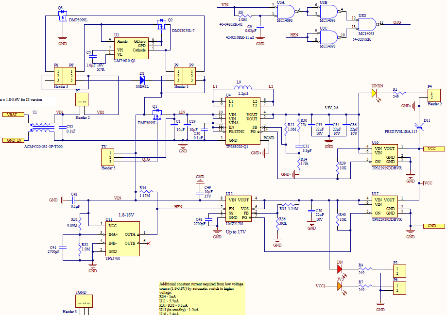
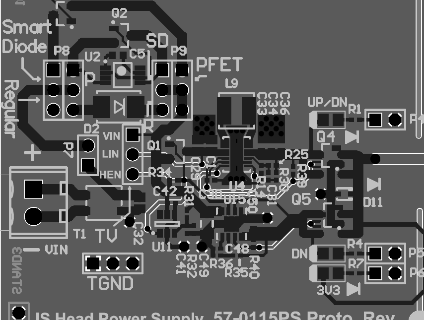
    Here are final schematic of my prototyping for the power supply and layout for this part. Schematic changed during debugging process, so, layout is for the previous rev, but layout for the DC/DC converters stay the same.

    The end application is a battery powered RF device (based on CC1200)  that should work from 3V alkaline battery that can go down to 1.8V or from 3.6V battery in Intrinsically safe mode or from 6-12V battery in non-IS mode.

    Unfortunately PDF files could not be uploaded :(

  • Unfortunately I could not find low power boost/buck converter working from 1.8 to 16-18 volts and tried to make combination of two. However, looks like this solution in Low Voltage mode is not low power at all. :(
  • It seems like you operate the TPS63020 in forced PWM mode.

    Could you try to connect the PS/Sync pin of the converter to GND and measure again the input current at no load?

  • Sabrina, thanks.
    After grounding this pin the zero load current became lower. goes from 38 to 70 µA