This thread has been locked.

If you have a related question, please click the "Ask a related question" button in the top right corner. The newly created question will be automatically linked to this question.

TPS6109 Not Boosting

Other Parts Discussed in Thread: TPS61090

Hello,

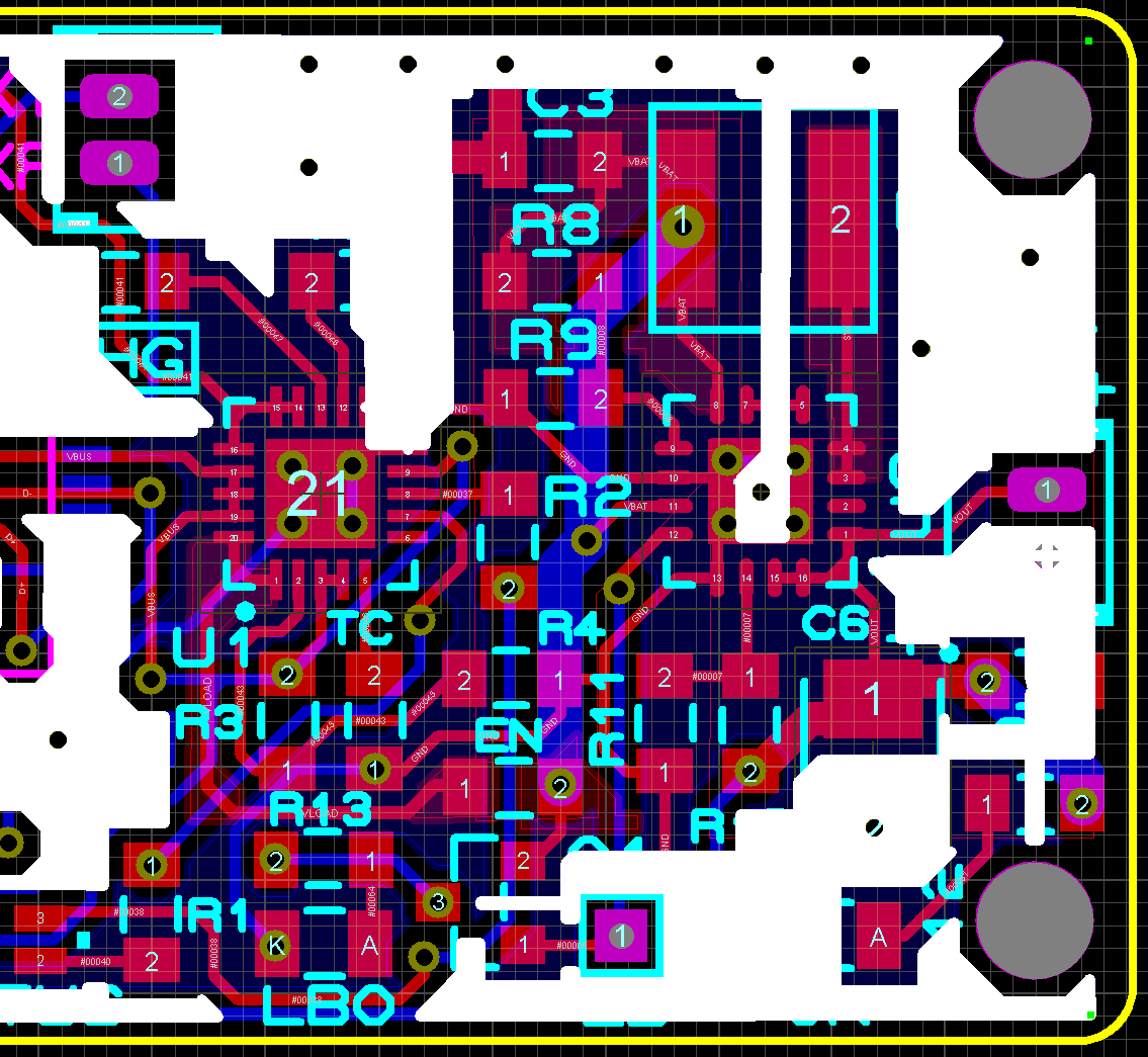
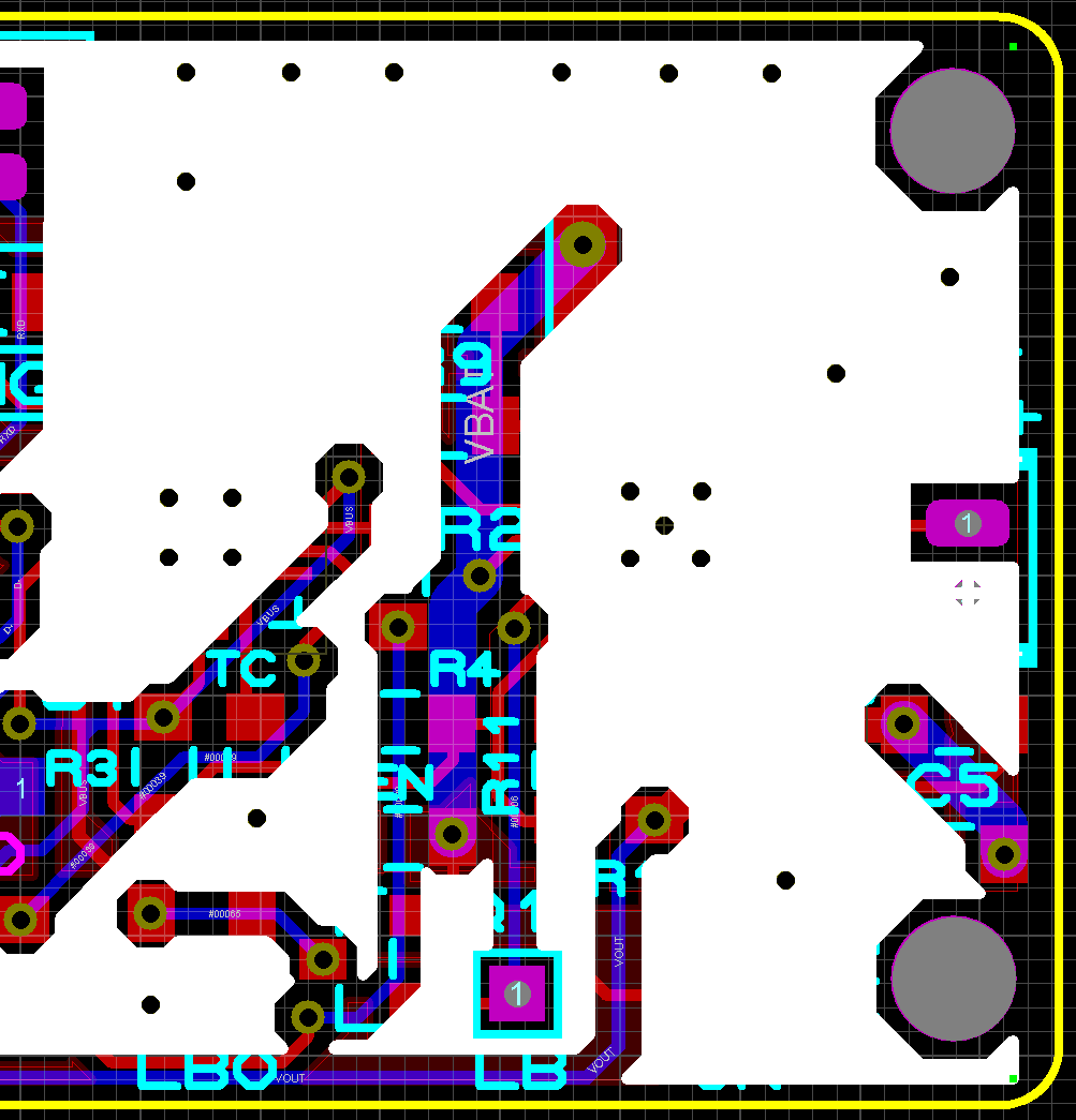
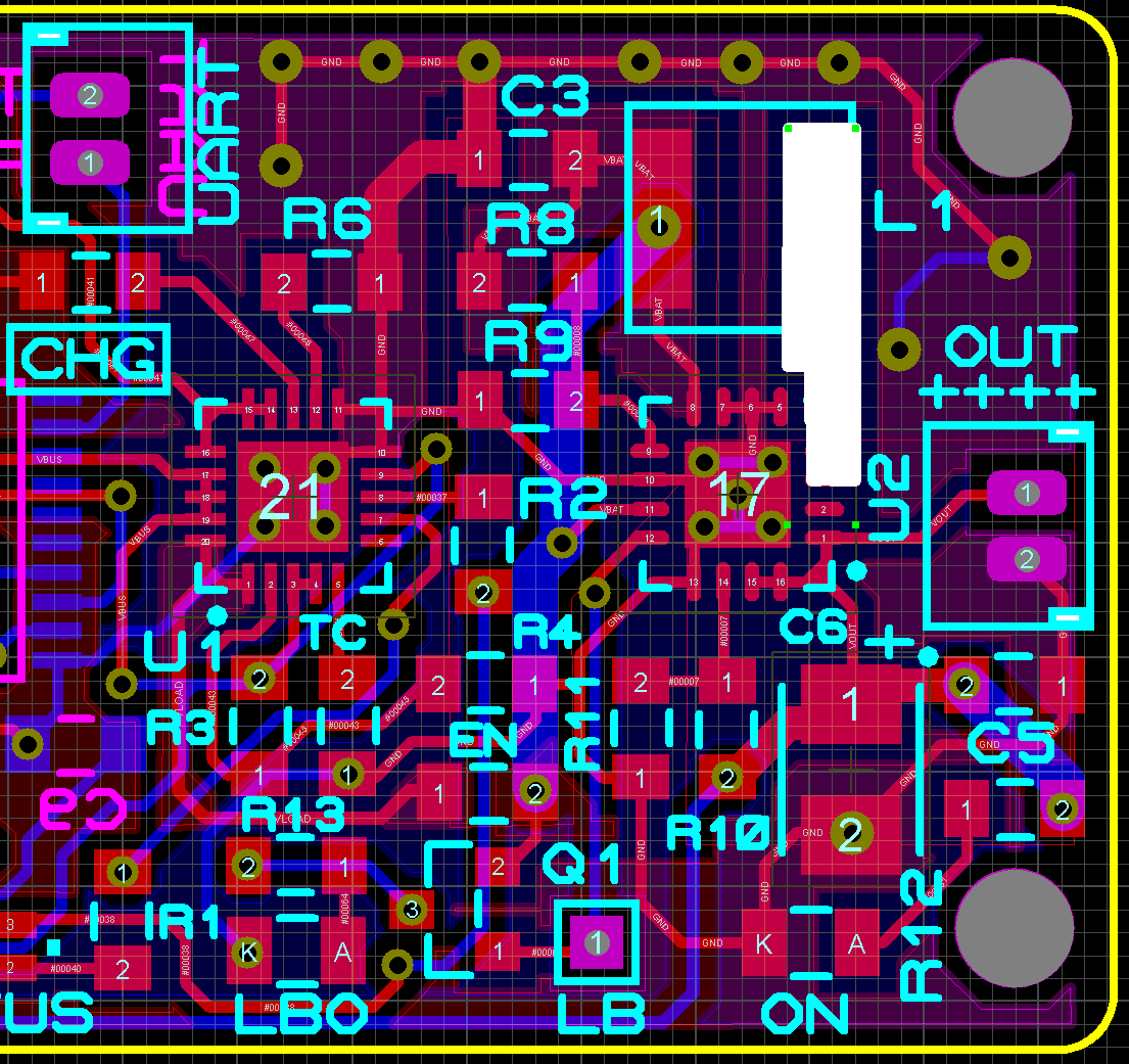
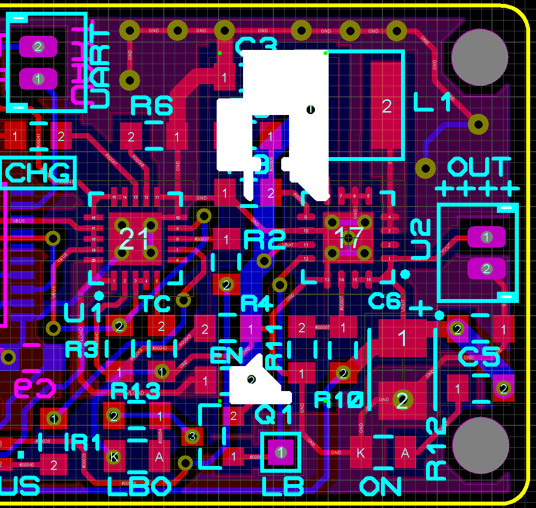
I am using a TPS6109 to boost to 5V from a 3.7V li-ion battery. My problem is that even with the TPS enable pulled high, the chip is not converting voltage.  I have attached schematic and board layout.  Any ideas what could be causing this?
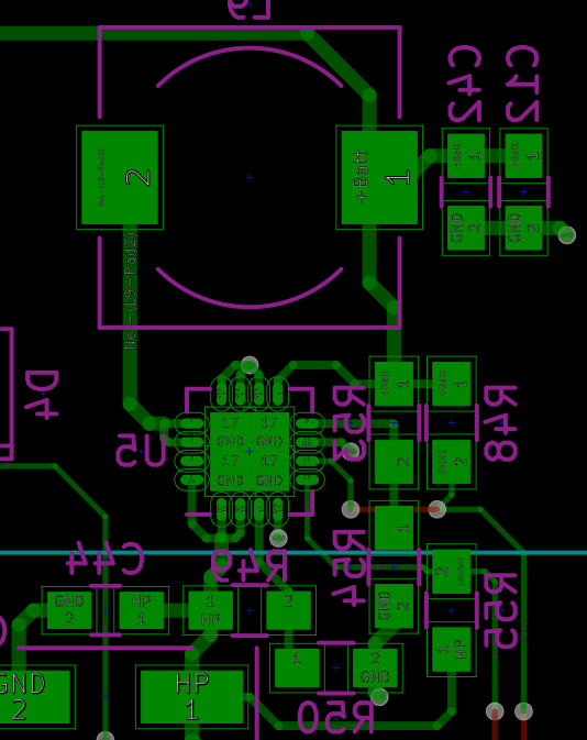
  • sorry for the late reply.
    i don't see problem in the schematic, but the layout is really bad. please refer to the datasheet page 19 and the application note "SLVA773" to modify the layout
  • Hello,

    We have designed a similar project issued from TPS61090 in order to generate +5V output from 1S Lipo Cell

    At the power-up the output is +5V and quickly turn down to 3.2V (after and 5s or 6s after Vbat is applied )  even there is almost no load on the OUTput .

    We took care about PCB design and we double checked it already, we still don't understand what is wrong.

    Any help or comment will be much appreciated.

    Here is our PCB with highlighted different parts of : TOP Ground Plane, Bottom Ground Plane, SW Plane and VBAT plane

    PCB

    TOP Ground Plane

    Bottom Ground Plane

    SW Plane


    VBAT plane


  • The layout is not good. there is risk that the device could get damage in heavy load condition.
    but I think it should be work at no load, or light load condition.
    1. can you observer the same problem in other boards?
    2. measure the resistance between the GND pin and other pins, to check if the device got damage
    3. measure the voltage level of every pins when power the device, to find if some pins are abnormal
  • Hello,

    This is a prototype we made, so we don't have other boards in service.

    Can you explain what is wrong with the layout ?

    We tried to inspire the PCB from the layout example shown in the datasheet.

    Our test has been done with a very light load connected : 1 led and 2,2 K resistor ( ~maximum 20 mA consumption ),

    The output voltage gets down to ~3,20 V within 2 or 3 seconds after startup.

    Could we find somewhere a PCB layout provided by TI that was tested working for TPS61090, then we should reproduce the layout.

    Regards,

  • The output ceramic capacitor should be placed closed to the IC, and the routing should be short. refer to datasheet page 19 and the application note "SLVA773". following are some steps to debug the problem
    1. apply an EVM for reference
    2. measure the resistance between the GND pin and other pins, to check if the device got damage
    3. measure the voltage level of every pins when power the device, to find if some pins are abnormal

    i would also suggest you can assemble another board, just the TPS61090 and its external components. it help to rule out the assembling problem or device damage.
  • Hello,

    The output ceramic capacitor should be placed closed to the IC

    C6 is the output capacitor, i don't see how we could place it closer from the IC.

    apply an EVM for reference

    Would you please provide much details regarding how to do this, this is not clear for us.

    measure the resistance between the GND pin and other pins, to check if the device got damage

    How many ohms should we expect to measure from GND pins to other pins ?

    measure the voltage level of every pins when power the device, to find if some pins are abnormal

    Please provide value we should find

    you can assemble another board, just the TPS61090 and its external components

    This is exactly what we did so far.

    Regards,

  • Hello,

    We build a new PCB and took care about advices you provided.

    Result is exactly the same, the output voltage turns down to 3.4V again after 5 seconds instead of sourcing 5V.

    The devices gets also very hot, it looks the temperature security is applied to secure it.

    * Could C6 be tantalium capacitor or must be ceramic ?

    - When we use 100uF tantalium capacitor for our tests, output voltage falls down after few seconds after the board power-up.

    - If we use 100uF ceramic capacitor, the voltage goes immediately at ~3.4V after the board power-up.

    * Is the PCB thickness important ?

    -> Our prototype has a PCB thickness= 1.2 mm

    * Note we only soldered TPS61090 and necessary peripheral components for our test.

    * Main source is a Lipo 1S cell.

    Any help will be much appreciated.

    Here is our latest PCB :

  • i still see problem in your layout, have you refer to the "SLVA773" to build the layout? i am think if i can make an TPS61090 pcb layout example for you.
    could you start a new post to summary your question? it is easy for me to miss your message in this post. i'll answer your questions one by one in the new post.