This thread has been locked.

If you have a related question, please click the "Ask a related question" button in the top right corner. The newly created question will be automatically linked to this question.

LM3671MF-ADJ Device Failure

Other Parts Discussed in Thread: LM3671

I saw another post with a similar situation as I had. I exchanged a few comments on this post, 

Mark has his Enable pin ties directly to Vin and so do I. I've built the 1st 2 prototypes and during testing I've had both board exhibit partial shorts. I just returned from a trip and was able to replace the LM3671 device. With failed deive removed and on the workbench I measure only 10.6 ohms between Vin and GND (pins 1 and 2).

The input source to this circuit is a 100mAh Li-ion battery and the load is a BT SOC and a sensor. The load is very small when I am running the board, less than 5mA on average but I guess the BT bursts are so short I do not see the current change on my bench power supply.

My schematic and board layout is in the other post but I was just able to take a scope shot of the switch node (pin 5). That looks like this:

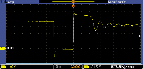
I'm not seeing the large -2.5V undershoot that was detailed in the other post. I believe that this signal looks good but I wanted to have it reviewed. I'm concerned that the 2 boards that I built both seem to have the LM3671 fail (I have only replaced the LM3671 on 1 board at this point). The other post talked about the switch pin shorted internally but my Vin pin seems to shorted to GND so maybe I have a different issue.

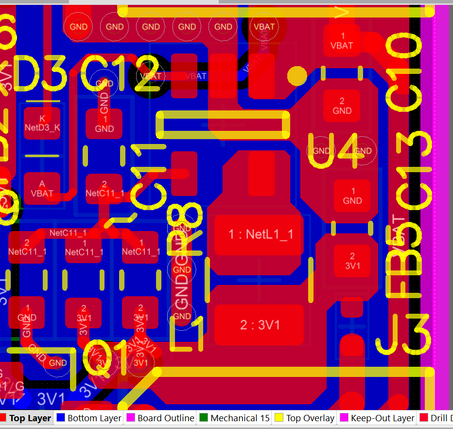
Here's my schematic and board layout:

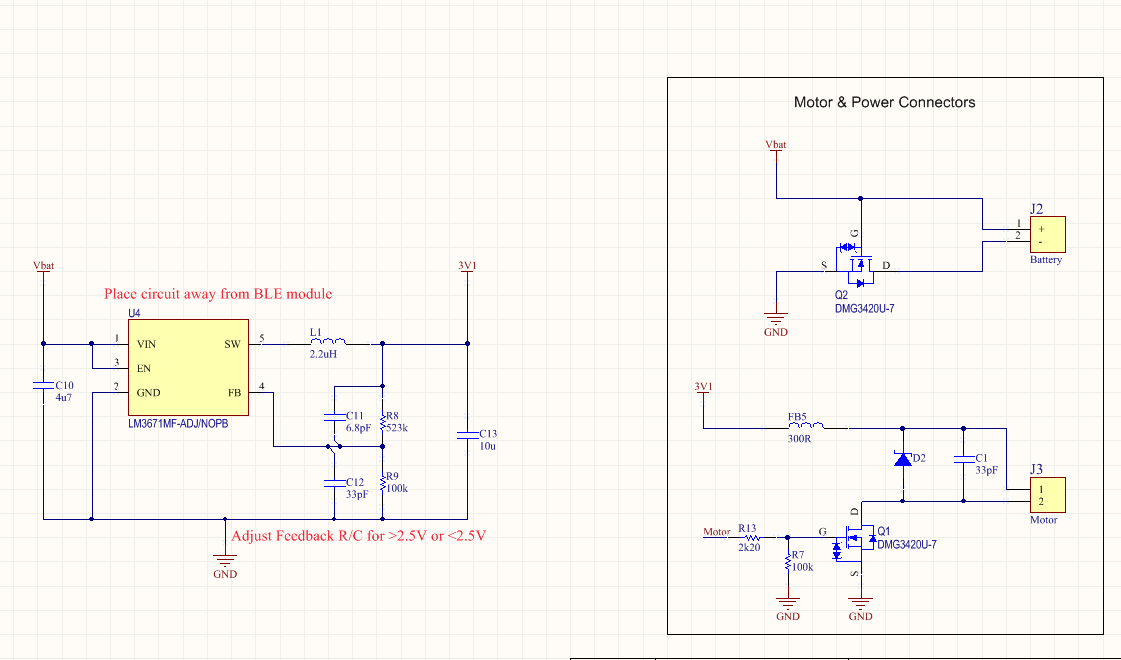
I see now that the feedback connection to the output (3V1) should not have been directed connected to the inductor so I may change that.

Is it still advisable to add a schottky diode the SW pin because I have the enable pin shorted to Vin? Since my failure mode is different and I don't (initially) see large over/undrshoot maybe I don't need to add the schottky.

I've got a tight production schedule that I can't miss so I only have a couple of days to determine what to do so any advice would be greatly appreciated.

Thanks,

George

  • Hi,

    the schematic and layout are looks good to me, except the feedback back network connection point which you already mentioned, move the joint close to the

    output cap/C13. I don't think the schottky is necessary. however, adding a small 100pf Cap in parallel with Cin/C10 is always to have. another suggestion is to

    enlarge the GNF island shared by CIN&COUT, adding two more vias to connect to the main GND layer. do you have any ESD/surge protection at power line? it's better

    to have one TVS diode if there is not. hope this can help..

    -Sheng

  • Hi Sheng,

    Thanks for reviewing. The board space is very tight (~1" x 1") so we couldn't make the ground area larger on the top layer. There's isn't any ESD protection on the input because this battery will not be user accessible. It will be installed during manufacturing and no direct access to it during use. There is the reverse protection MOSFET on the ground line of the battery so that provides some protection.

    Right now I'm very concerned about my 2 boards having failing LM3671 regulators. There wasn't anything during testing that I can recall which would have caused a short. I've replaced one regulator successfully and I'll have both boards inspected this afternoon for any hidden trouble but I haven't been able to see anything on the board.

    Thanks,

    George

  • George,
    In this case, I would recommend to return these two failure parts back to TI for a FA analysis, so we can have a clue of what's the cause.

    -Sheng
  • Sheng,

    Can someone PM me with some details or a contact with an engineer in this group. I'm going through the standard sales channel but my timeline can't afford the "normal" route. I already have a 7k order for these parts so I need some quick action since production is supposed to start in 30 days.

    Thanks,
    George
  • Lutz, Andy <Andy.Lutz@ti.com> is the CQE, who may be able to help.