This thread has been locked.

If you have a related question, please click the "Ask a related question" button in the top right corner. The newly created question will be automatically linked to this question.

VCC & input signal timing requirement on UCC3915DP

Other Parts Discussed in Thread: UCC3915

Hello,

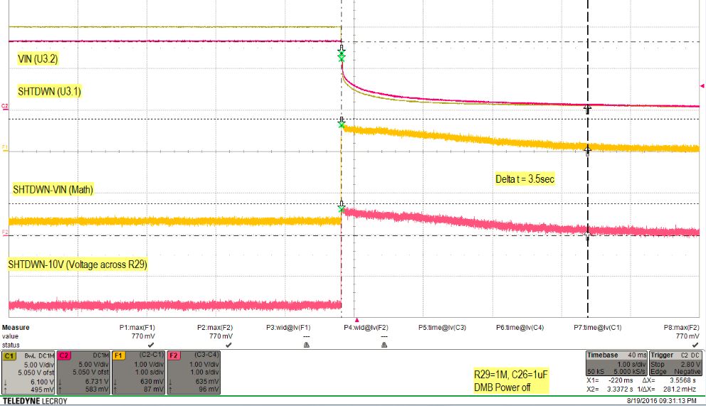
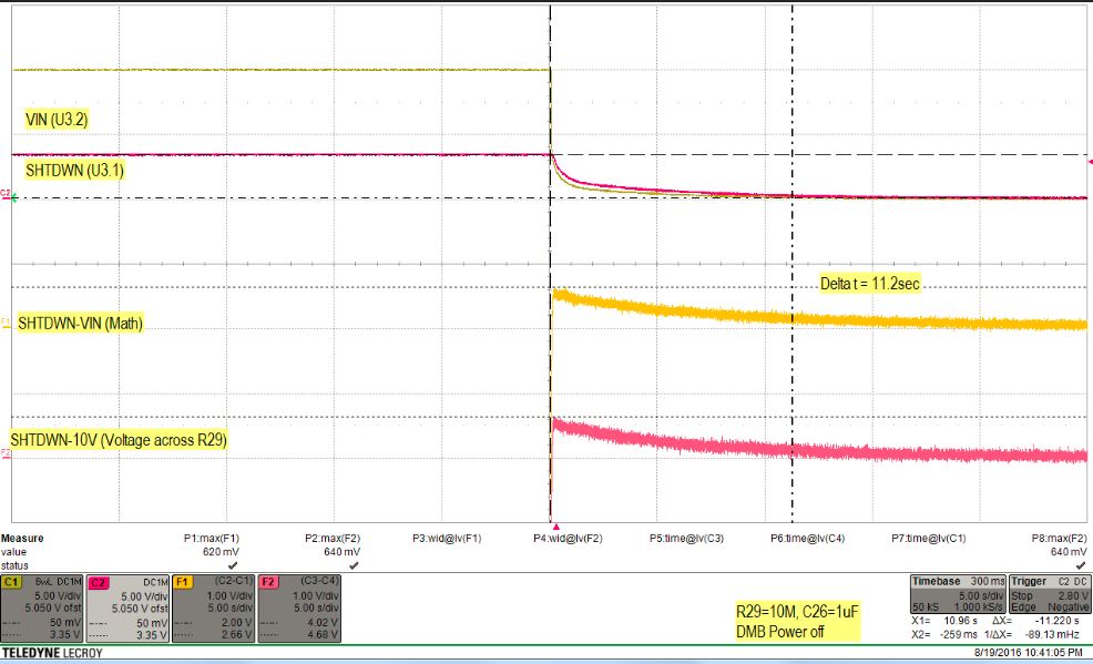
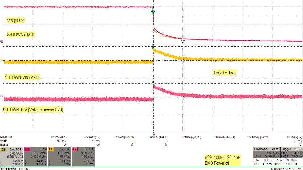
Is there any time sequencing between " Vin" (Pin 2,3)  &  SHTDWN (Pin 1) to be followed for UCC3915DP ?

As per datasheet of UCC3915DP , recommended operating voltage is 7V to 15V  and threshold for SHUTDWN pin is 1.5V typical.

In our present design signal on SHTDWN pin appears around 100ms before VIN arrives at 7V. Will there be any issue with this condition?

Does this scenario lead to latch-up of IC  or will there be reliability risk ?

Thankyou

  • Prakash,

    Welcome to E2E. Intially, I would say there is no issue. Will require a little deeper look and may take a day or two to get a definitive answer.

    Brian
  • Hi Brian,

    Can you please take a deeper look on the above concern? This chip will be used on a critical life support system. As per the information that we received in past (2011) from Ti, the scenario of SHTDWN signal arriving earlier than VIN will violate the datasheet requirement of "TTL input voltage : –0.3 to VIN" which could possible lead to Latch-up condition (between VIN & SHTDWN).

    The requirement of -0.3 to VIN is only for continuous operation or even for a short duration of ~100 to 200ms ? ( this delay is due to ramp up of input voltage VIN). Though we are providing both VIN & SHTDWN from same source, the thresholds for VIN & SHTDWN are different (7V min & 1.1V min for VIN & SHTDWN respectively)

    Were there any improvements done to "UCC3915DP" chip past 2011 ?

    Kindly share your inputs at the earliest.


    Thanks & Regards,
    Prakash.S.R
  • Prakash,

    /SHTDWN will fall under the DS TTL line for absolute max rating.  There is a diode from /SHTDWN to Vin that if Vin is lower voltage than /SHTDWN, there will be backfeed into Vin that could cause UCC3915 failure.  So /SHTDWN must be lower voltage than Vin.  I think you may be describing ramp up voltages on both.  As long a you meet the -0.3v to Vin, even with Vin ramping, this diode will not conduct and there should be no problem.  You should test for expected results, as always, especially given the nature of your design use.  It is recommended that you use a transistor, like S6 in the DS diagram, to control /SHTDWN with and external control.  

    Consider checking the "Verify Answer" button if I've answered the question to your satisfaction.

    Brian

  • Hi Brian,

    During turn-off sequence the voltage on the VIN of UCC3915 falls below 5V almost instantly but on the  /SHTDWN pin there is an RC of 976K & 15uF, which will delay the fall of voltage. The condition of  -0.3v to Vin will be violated for over 1.5 sec. Will there be any issue if /SHTDWN has momentary higher voltage than VIN during power down sequence ? Will this still cause the diode between VIN & SHTDWN to conduct ?

    Thanks & Regards,

    Prakash.S.R

  • Prakash,

    If the capacitor were a small value (like 0.1uF), then the energy would likely be absorbed without issue by the internal diode (maybe with a 20ohm series resistor with the cap to limit peak current) from /SHTDWN to Vin. Given 15uF is used, the likelihood of this energy being too great is there. I would recommend a transistor pull down be used (S6), with comparator control to acheive the desired long turn on delay.

    Brian
  • Hi Brian,

    I had previously attached screen shot of schematic and waveform in the previous post (Aug 5) using "upload from word" option. Were you able to go through the same ? I do not see the schematic being attached in the post, so can you please conform ?

    Thankyou.
  • Prakash,

    Did not see a schematic in this thread. Was a schematic in a July thread.  I believe that there is too much energy in a 15uF capacitor on the /SHUTDWN pin that can potentially discharge with very high peak current into the UCC3915 through the diode from /SHUTDWN to Vin that could result in UCC3915 failure.  The best solution would be to have a clean comparator input to the /SHUTDWN pin with all timing taken care of prior to the comparator and small, if any capacitance directly on the shutdown pin.  The UCC3915 fig 1 shows the RC but in no way would the IC have been tested with such a large capacitor so this is uncharted territory.  If a comparator is not an option, maybe you can look at a Schottky + small resistor in parallel with the 976k resistor as a fast discharge path while retaining the desired long turn on delay.  You may want a small resistor (10 ohm or so) in series with the capacitor as a peak current limiter and to absorb discharge energy, just in case some current is directed to the /SHUTDWN pin to Vin.  Of course, all this needs to be fully proven in during your product qualification.  These are suggestions to try and are not guaranteed as a full solution.  See attached.

    Brian   Ti Support_older thread.docx  

  • Thank you Brian for all the support.
  • Hi Brian,

    A small update. We retained C26 @ 1uF as per schematic that was shared last time, but we varied R29 to 1K, 100K, 1M & 10M....What we observed was that discharge time for C26 from SHTDWN pin (during power-off sequence) was incremental with R29.....That means to say, Most of the energy on the cap C26 was discharging through R29 rather than through SHTDWN pin of IC. This could be because of very high input impedance on SHTDWN pin, which will not allow much energy to dissipate through SPL IC. Also the max voltage difference between VIN & SHTDWN is 0.7V. (could this be diode action?)

    (we do not have option to modify PCB, hence we are trying possible options. We will surely consider your previous suggestion of diode in future)

    Please go through below waveforms.

    With this can we say that energy dissipated into SPL IC through C26 is minimal and is discharged through external resistor R29 to 10V rail ?

    Will it be possible to provide input impedance of SHTDWN pin & max energy or current that can be handled by internal diode on SHTDWN pin (As per your previous post) ?


    Thankyou for your time on supporting us.

    Can you share us your contact info, if possible?  So that we shall have a meeting to understand better on this issue, rather than sharing details through post.

  • Prakesh,UCC3915 Evaluation board slua187.pdf

    The leading edge of the pull down of Vshtdwn is an area to look into carefull.  With 1 to 5 seconds/division resolution, little info is shown on the plots in this region.  Vshtdwn looks to pull rapidly with Vin as the diode between the 2 pins is conducting/clamping, much faster than the RC TC of R29/C26.  Then it appears POR on downstream devices shut reduces the load current and dramaticaly slows the Vin decay from what ever bulk capacitance is present and the difference between the two pins is related to the 100ms and 1 sec RC TC and the final decay of Vin.

    1)  Recommend you put a current probe between the 2 pins and measure the actual current being conducted between SHTDWN and Vin.  Measure the leading edge and the sustained portions.

    2)  If Vin were shorted, the peak current from the capacitor would be high.  In the scope shot, it looks as though Vin is simply shutdown.  I don't know if this is a concern or not, but a shorted Vin would place high energy over a very short time on the diode.

    3) Normal input impedance of the SHTDWN pin is very high as it will draw 0.5uA at 12v.  However, once Vshutdown > Vin, the data sheet violation noted as your concern, then the protection diode will conduct with low resulting impedance.  This is an ESD device that is intended for low energy human body discharge, not sustained currents.  If the current probe measurement exceeds 100mA peak, a latch up conditon can occur.  If ~ 10mA sustained (untested duration of 'sustained') then diode failure may be possible. Either way, this still violates the DS specficaiton and cannot be supported by TI but is provided for your use and risk assessment.

    4) My recommendation would be to bite the bullet and relayout the pcb with the recommendations noted earlier in the email. If you have units built, I would tack on the components to the existing circuit board, ugly as it is.

    5) See attached evaluation board.  I don't think it is manufactured still, it was a late 1990's design.  The Shutdown cap is 0.01uF and I'm sure this was how all of the testing was done by one of the great analog Engineers the industry has ever seen (see author).  Unknown what the pull up is but it looks like a resistor bank, likely 10k. 0.01uF is what we have some history with, but again, likely a 10k or less pull up resistor.

    6) However, if Vshtdown exceeds Vin, i.e. the DS is violated, TI cannot support doing so and risk assessment is up to you through a thorough product qualification.

    Brian