This thread has been locked.

If you have a related question, please click the "Ask a related question" button in the top right corner. The newly created question will be automatically linked to this question.

TPS6300x PGND / GND

Other Parts Discussed in Thread: TPS63000, BQ27510-G3, BQ24210, BQ27510, ULN2003LV, PMP9768

Hello,


I'm working on a complete charger / gauge / regulator +3.3V and +5.0V design (with the Fuel Tank BoosterPack taking as a working basis).

My questions :


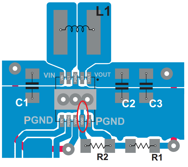
1) I have a misunderstanding between the schema of this card and the recommanded layout in the datasheet of the TPS6300x about the PGND.
 It is recommanded to have a power ground different from ground but in the boosterpack schema, GND and PGND are not separated : there's only one ground : GND. Why ? Isn't it a problem ?

2) With Google, i can find schemas with only TPS6300x and good separation of GND and PGND, but i never find schema with TPS6300x integrated in a full circuit (with other functional blocks) with separated grounds. I would like to find a full circuit (or partial schema / PCB) with a TPS6300x, separated GND and PGND, and other blocks as a source of ideas because i don't exactly know how to use this different grounds with my other components (i have LiPo charging and gauging blocks, and OLED screen, microSD card...). Do you have an example of good practice layout like the boosterpack but which respects the datasheets' recommandations ?

Hope my questions are clear :-)

Thank you.

Christophe

  • As stated in the datasheet of the TPS63000, we recommend to separate PGND and GND, to avoid noise related issue, as PGND is more noisy than the GND. But ultimately they are tied together in the layout, that may be the reason they named it the same way,

    In the picture below, you have the layout recommendation (from the datasheet) where the PGND and GND are overall separated but are tied only at the device with a net-tie (circled in red).

    I don't know which boosterpack schematic you refer to but I would recommend to follow this layout for the power stage. I would suggest to do your  layout  and  send it to me for reviewing as well as the schematic.

    I would also recommend you to take a look at the TPS63000 EVM User's guide to have a comprehensive overview of the circuit:  http://www.ti.com/lit/ug/slvu156/slvu156.pdf 

  • Thank you for your answer.

    The TI's boosterpack is here : http://www.ti.com/lit/ug/slvua32/slvua32.pdf

    I'd like to respect the layout of the datasheet in my design. But I'm at a little bit of a loss to integrate this design in my full circuit with a BQ24210 and a BQ27510-G3 : i'd like to have confirmation that my components are connected to the correct grounds each time.

    Here a part of my design :

    My interrogations are : how can i be sure when i must connect a pin or a component on the PGND or on the GND ? For example, in the datasheet of the TPS63000, it is mentionned to connect the pins VIN and VINA to the GND (and not the PGND) with a resistor. So i ask myself for my BQ27510 (for example) if how i must connect the different pins (for example the TS pin, or the SRN pin) ? Does my sink driver (ULN2003LV) must be connected to the PGND ?

    So many questions... That's why i'm looking for a full design example.

  • I would  follow the layout recommendation  of the datasheet for each component.  I would do the layout for each circuit as islands and have a common ground on a separate layer for the system as a whole. You could take a look at the reference design to give you an idea how this would look like:  "PMP9768 - Automotive eCal power supply reference design with high intermediate voltage"  ( http://www.ti.com/tool/PMP9768.1?keyMatch=null&tisearch=tidesigns&keyMatch=PMP9768&tisearch=Search-EN-Everything )

    Ror example if the sink driver is is supplied by the TPS63000 then it sould be connected to the power ground.

    Again these are suggestions from my side,  the layout of course depend on your whole system,  what is the application behind? 

    How did you choose this converter? What is your Vin, Vout, and load condition? 

  • Hello,


    Thank you very much for your link !

    I notice that my image in my last post hadn't been uploaded. So here, a part of my design :

    As you will see, it is derived from the fuel tank boostpack, but with a dedicated power ground to respect the layout of the datasheet.

    At the beginning, i have studied the MSP430TM Based Lithium-Ion Polymer Battery Charging and Gauging Solution Using USB Power (SLAA529A document) but, after, i have discover the Fuel Tank BoosterPack and found the schema and PCB design, so i decided to follow this design for mine. But forward, i think i will follow the SLAA529A layout).

    My whole system is made up of an MSP430 (3.3V), an SDCard(3.3V), an oled screen(3.3V), a fingerprint module(5V) and some buttons. Not complicated so, and must imperatively be autonomous, that's why i must use a LiPo battery with charger module, gauging and regulators (3.3V and 5V). The whole system will consume less than 400mA, so the TPS6300x is correctly sized to be used with (or the TPS6303x a bit less expensive).

    There is also an ULN2003LV to drive the peripherals from the MSP430. The ULN2003LV is connected to the PGND. The VSS of each peripheral is connected to the ULN2003LV, so, to the PGND when "turned on".

    My questions are about the other modules :

    - Buttons are connected to the GND,

    - Cristals are connected to the GND,

    - MSP430 is connected to PGND.

    Are my charging and gauging modules correctly connected to the ground ?

    Is there a rule or good practice to know when to use the ground rather than other ?

    Many questions but i'm progressing ! :-)