


Hi everyone,
I'm designing a power block and I have a look LM5117 Evaluation Board.
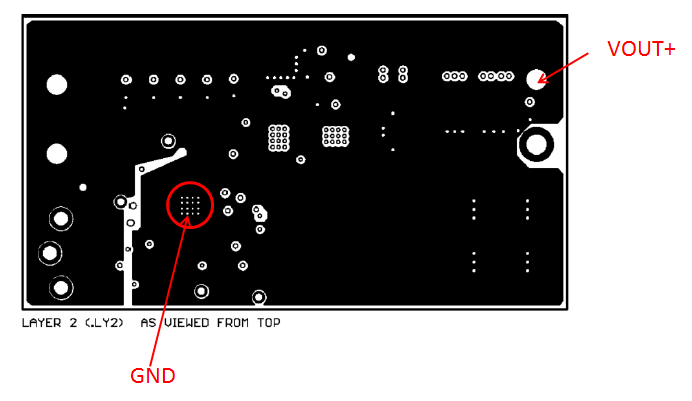
I find PCB layout on the LM5117_AN.pdf and there are some questions.
Are the layer-2 and layer-3 GND layer?
The chips' thermal vias(GND) are connected to a copper but VOUT+ pin also is connected to the copper.
Please find attached picture.
Can you please advise the copper net name or provide a gerber fiel?
Thanks and regards,

