


Dear e2e,
on behalf of my customer where the currently design a AC/DC converter with a bridgeless PFC circuit in the first stage, I'd appreciate if you could comment to the questions at the end of this post.
Best regards,
Uli
===================================================
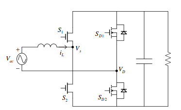
The converter is based on GaN FETs and will deploy approximately 400kHz (T=2500ns) for the PFC stage.
Active snubbers will reduce the switching losses for S1 and S2 (not shown in the drawing).
We need to create the following signals:
a) PWM for S1 and S2 dependant on
- The current through the main inductor
- The actual voltage at L and N (we will sample both voltages to GND individually)
- The dc voltage across the capacitor
- Perhaps the load (although just regulating the capacitor voltage might be enough)
- The time presently set for the active snubber (see b))
The role of S1 and S2 changes at each half wave sine. For positive half waves, S2 is the "leading" switch, S1 is the freewheel switch. For negative half waves, it is the other way round.
I would like to implement a cycle-by-cycle short-circuit protection.
When the input voltage approaches zero, I would like to reduce the PWM as far as possible and switch it totally off for a short while. Than it should soft-start at the next cycle.
b) The active snubber signal
Prior to activating the main switch, we need to activate the active snubber of that main switch (S2 for positive half waves, S1 for negative half waves).
The active snubber needs approximately 160ns at full load, but this depends on the present current through the main inductor (the smaller the current, the shorter is the time needed for the active snubber).
So the active snubber depends on
- The current through the main inductor L
- The dc voltage across the capacitor (should only be important for start-up, but we need to consider it anyway)
c) The control signals for the active rectifiers SD1 and SD2
This is the simple part. For positive half waves, SD2 needs to be activated, for negative half waves, SD1.
So the signals for a) and b) look like
a) S1 ------x___________x-----------------------------------x___________x-----...
S2 _________x--------x______________________________________x--------x_____...
b) S1 ________________________________________________________________________...
S2 ______x--x____________________________________________x--x______________...
"x" means a configurable dead time. The dead time might be different for the transition from a) to b) and from b) to a) and between a).
Please bear in mind that the active time for b) is dependant on the present current through L.
Ideally, the controller would first calculate the present required duty cycle and then subtract the time required for the active snubber.
My questions are:
1.) Can we use the UCD3138 for this task and in which configuration?
2.) Would we have to implement the transition between the half waves in software? That would mean a reconfiguration of the hardware every 10ms (50Hz) or 8.3ms (60Hz).
3.) Can we create the active snubber signals dependant on the input current and bridge voltage, if so in which resolution (4ns or 250ps)?
4.) Can we use different dead times between the signals? What is the resolution for the dead times (4ns or 250ps)?
===================================================