This thread has been locked.

If you have a related question, please click the "Ask a related question" button in the top right corner. The newly created question will be automatically linked to this question.

TPS650832 VCCIO Enable Signal

Other Parts Discussed in Thread: TPS650832

Customer's question on the datasheet diagrams for application diagram and sequence timings.

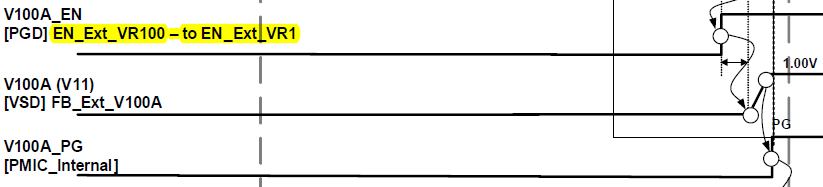
From the system block diagram of TPS650832, the V100A is the output of internal VR1, and VCCIO is the output from external VR7.


But Timing Diagram shows the V100A is Enabled by External VR1, and VCCIO is enabled by internal VR1, this is confused to customer. Is this a typo error?

Or could you please help to add some comments on that? Thanks!


V100A


VCCIO


  • Answer: Yes, this is a typo in the datasheet. Thanks for catching it and pointing it out. We will get this fixed.

    V1.00A is supplied from VR1 and VCCIO is supplied from an external buck like TPS62134x. V1.00A is enabled when ENVR1 is asserted high. VCCIO is enabled by connecting the PGD pin on the PMIC to the EN pin on the discrete buck. The PMIC decides to enable VCCIO in the proper sequence order or when the user requests an over ride of the sequence via I2C.