Hello guys,
Our customer has the following questions about LM3463. I checked LM3463 datasheet but I couldn't find the answers. If these questions are solved, they will start to evaluate this device.
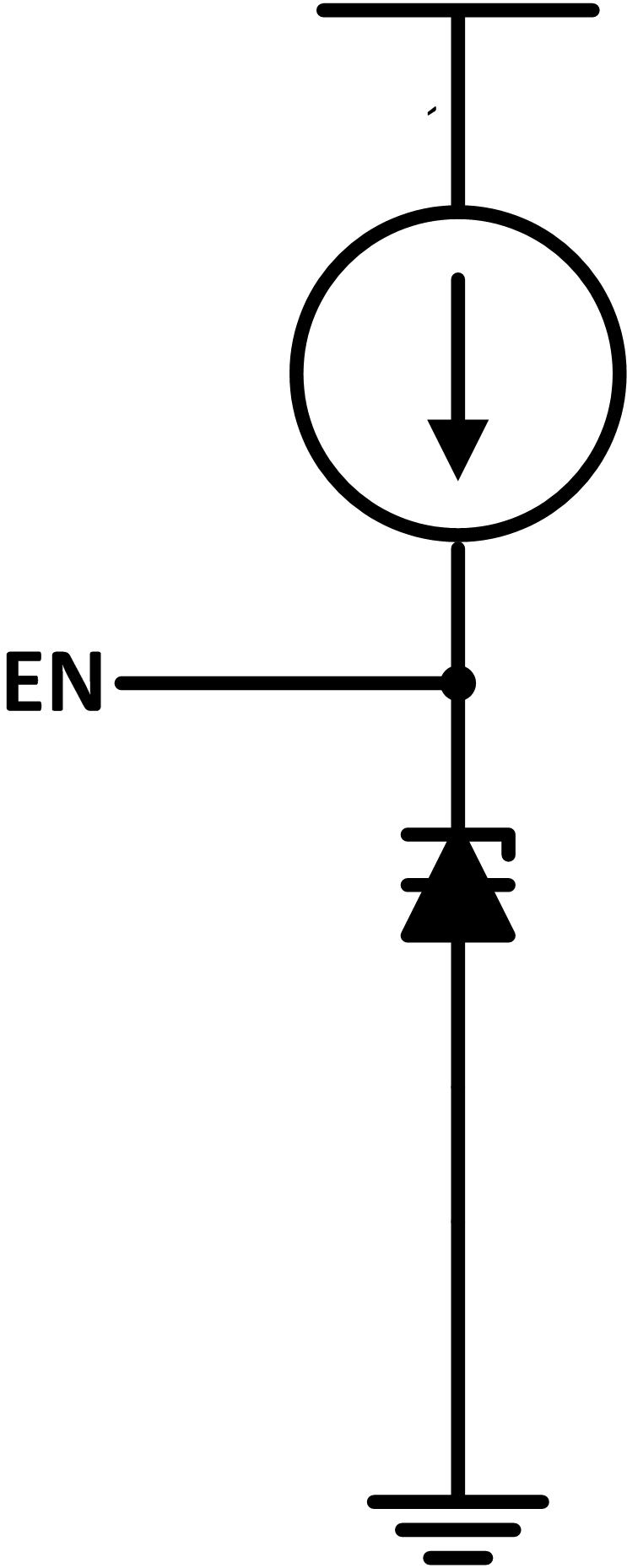
1. What voltage is the internal pull-up of EN pin connected to? Is it VCC voltage?
If so, I think EN pin is charged up to 6.76V. Is my understanding correct?
2. What is the pull-up resistance of the EN pin?
3. Is there any block diagram or equivalent circuit of EN pin portion?
4. Is there any open drain CMOS logic IC which can drive the EN pin directly?
I checked SN74LVC1G07 (Single Buffer/Driver With Open-Drain Output) datasheet
and I found the recommended maximum voltage of open drain output is 5.5V.
So the logic device can 't be used for EN pin driving.
5. Is there any CMOS buffer logic IC which can drive the DIM01/DIM23 pin directly?
I checked SN74AUP1G17(LOW-POWER SINGLE SCHMITT-TRIGGER BUFFER) datasheet
and I think the logic IC can drive DM01/DM23 directly at 3.3V because LM3463 DM01/DM23 pin
input high level voltage threshold is 1.75V as the maximum.
6. Is the power supply of the DIM01/DIM23 input buffer VCC?
7. If the answer for No.6 question is yes, I think a few current leaking from VCC at DIM01DIM23
input buffer when 3.3V is applied to DIM01/23 because the input voltage is not VCC and is not full
swing. Then is VIN shut down current increased?
8. Is there any block diagram or equivalent circuit of DM01/DIM23 pin portion?
Your reply would be appreciated,
Best regards,
Kazuya Nakai.


