This thread has been locked.

If you have a related question, please click the "Ask a related question" button in the top right corner. The newly created question will be automatically linked to this question.

LM25116, too much noise on Vout

Other Parts Discussed in Thread: LM25116

Hello


I've to redesign old DC/DC modules containing Simple-Switcher controller. The goal is to achive a much better efficiency.

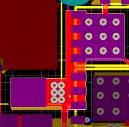
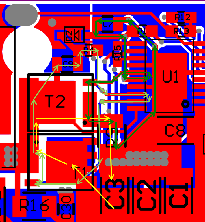
The device work properly so far, except I've problems with the HF noise on Vout. Due to the layout, I think.

I've compared it with the eval board, but haven't any idea.

Could some one look over it and give me some hints?

Schematic:

LM25116_schematic.pdf

Layout:

175063_A_layout.pdf

Some waveforms:

TN16081101_Spikes_on_175063A.pdf

  • Hello Juerg,

    The output spikes are coincident with the rising/falling edges of the SW node voltage. I notice there is no output cap near your output connection and your VOUT and GND connections are spaced far apart. Here are some other recommnedations:

    Minimize area of SW node copper

    Increase R4 to slow down T1's turn-on

    Install R16 and C30 RC snubber components (e.g. 2R2 and 100pF)

    Place solid GND plane on layer 2 immediately undereanth the top layer (i.e. immediately below power stage components).

    For more information, please review my article series on PCB layout:

    DC/DC Converter PCB Layout

    Regards,

    Tim

  • Hello Tim

    Unfortunately, the pinning is not changeable. But a cap from +output to the GND of Cin improves it. But it is difficult to route the GND back to Cin.

    I have tried via GND plane, it made it worse. Maby a cutted plane, separate from the IC would be better?

    I also increased R4 in steps until 39R, also helps.

    A snubber i had already before, but a much greater cap, i.e. 4n7. If I reduce it, the spikes increase.

    GND plane. Do I understand it correct? GND plane under T1 and T2?

    I saw on different demo boards from TI congruent SW node on all 4 layers.

    I do not see, how I can minimize the SW node. Do you think, it is to large?

    I have analysed the loops.

    • Switching power loop in yellow
    • Highside gate loop in light green
    • Lowside gate loop in dark green

    Do you think, they are to long?

    Best regards

    Juerg

  • Juerg,

    I think the layout you provided is okay.

    As Tim mentioned, adding a snubber and a gate resistor to the high-side FET usually help with output noise.

    Another way to help reduce high frequency noise is to add small value ceramic capacitors to the ouput capacitance. Values like 100nF and down help with this high frequency noise.

    -Garrett