This thread has been locked.

If you have a related question, please click the "Ask a related question" button in the top right corner. The newly created question will be automatically linked to this question.

BQ24650 - IC at CHARGE IN PROGRESS state but no charge current

Other Parts Discussed in Thread: BQ24650, LMP8601

Hi,

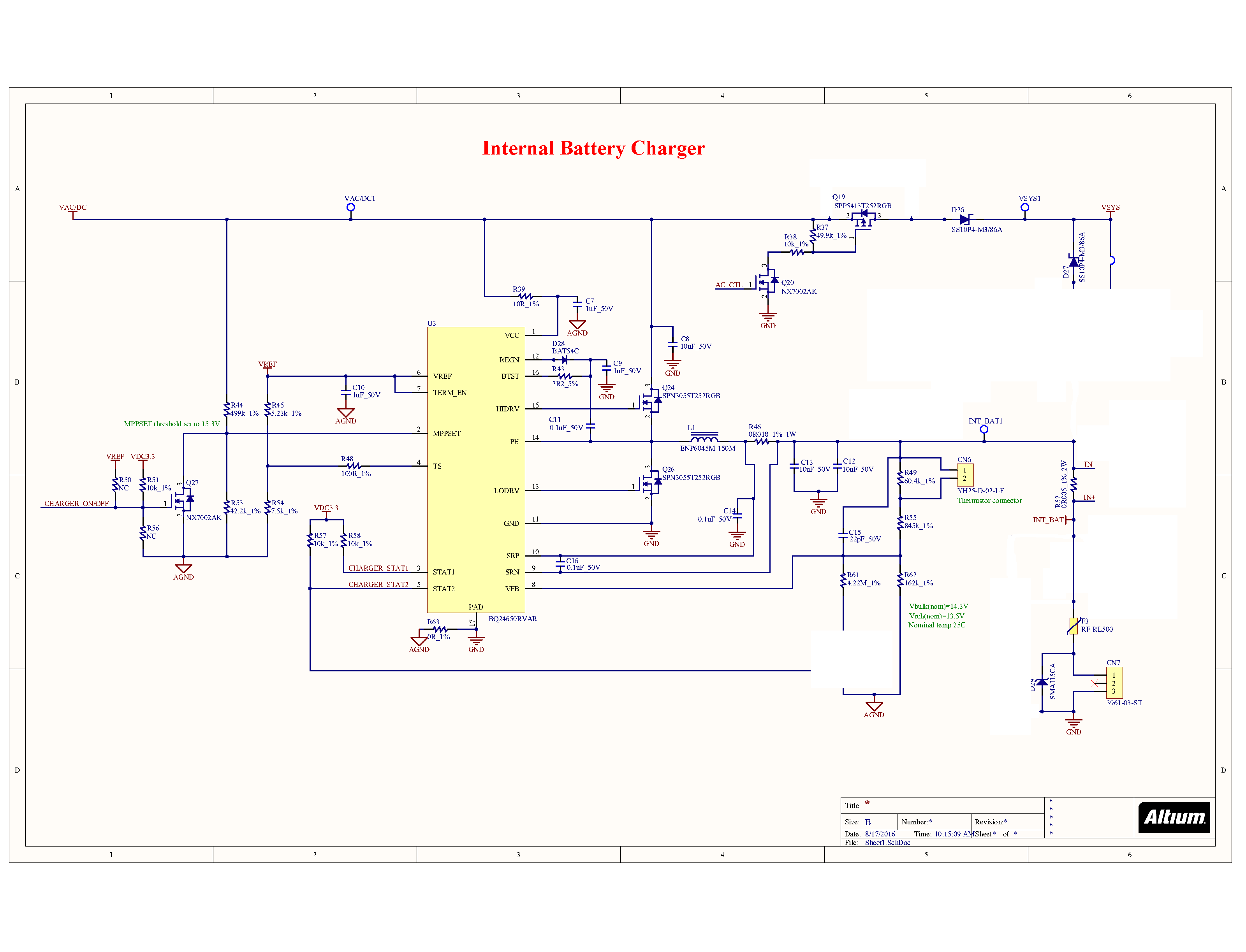
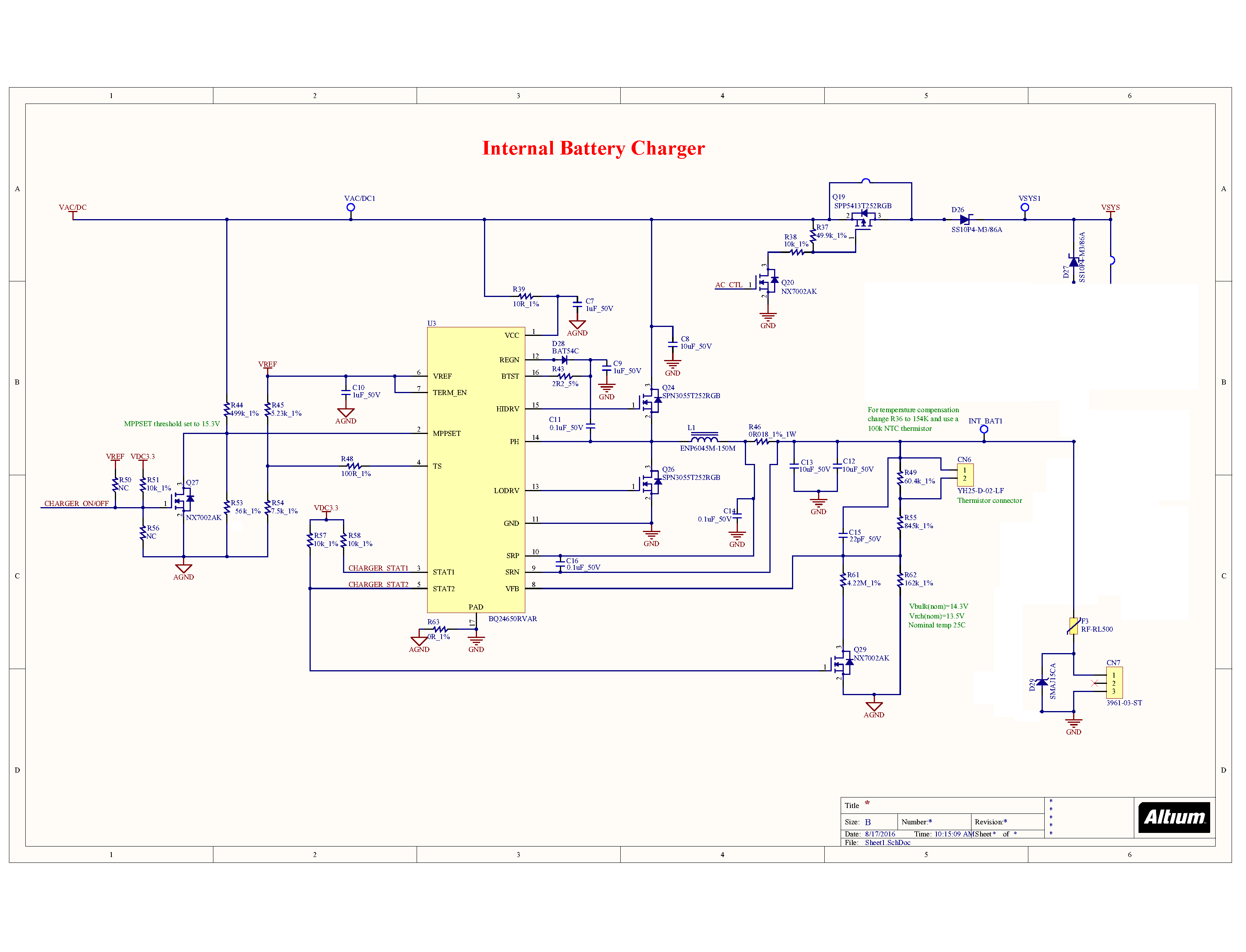
I implemented a lead acid battery charger using the BQ24650 as explain in the application note slva437a, testing the board I made it seems the charger should be working but I measure no current flowing into the battery. Let me explain, we have and MCU connected to the BQ24650 detecting the STAT1 and STAT2 pin, we are detecting the STAT1 at 0V and STAT2 at 3.3V which means the STAT1 transistor is ON and the STAT2 transistor is OFF.

According to the data sheet this means CHARGE IN PROGRESS, this is expected since the TS pin is at 1.95V, MPPSET is at 1.27V and VFB is at 1.56V. This means the charger should be at pre-charge. Since our current sense resistor is 18mOhm, the pre-charge current should be set to 220mA but I am measuring 0A. 

If I turn OFF the charger IC, by setting MPPSET pin to 0V, the STAT1 and STAST2 both return OFF which is the expected result. Turning the charger ON again give the same result, CHARGE IN PROGRESS but no charge current.

What could be the problem?

Regards

Mark

  • Hi Mark,

    Could you tell me what your battery charging voltage is, as well as possibly provide a schematic? That will help with the troubleshooting process.
  • Hi,

    The battery bulk voltage is set to 14.3V and the recharge voltage to 13.5V, down you can find the schematic. Please do not pay attention to the transistor Q19, Q21 and Q22 circuit, those are meant to connect either input power source (AC or battery) to the system. As you can see the only difference between my schematic and the one shown in the data sheet is that I am not using the reverse polarity diode since my input is not a solar panel, it is a AC adapter that cannot be plugged backwards.

    Today we modify the resistor divider connected to the MPPSET pin, with the modification we made we increase the MPPSET voltage to 1.5V and still the charger does not work.

    Hope you can help me to find the problem.

    Regards

  • Hi,

    Today we did more tests over the circuit, below you can find the schematic that reflect the changes we did. As you can see we try to isolate the charger circuit and the battery removing all other components that does not belong to the original application circuit.  Even with all those changes we got the same result. For a reason we cannot understand as soon as the charger is turned ON the battery pin has a voltage of 1.8V all the time, this in turn makes the IC detect a battery even when is not connected. This because the second condition of the battery detection sequence is met, when the charge current of 125mA is applied the VFB voltage never reach Vrech,stays at 1.8V, thus the IC detects a battery and report a CHARGE IN PROGRESS state (STAT1=OFF, STAT2=ON).

    Besides that with or without battery connected to the board the IC always detects a battery, in neither case it supplies a charge current. We honestly run out of ideas to test and it would be great that TI support team can help us in finding the root cause, this PCB is meant to be used in an important project and we are running out of time. Regards

  • Hi Mark,

    Sorry for the delayed  response. In response to your previous post, I was going to ask:

    1) can you verify your input voltage?
    2) can you verify VCC pin voltage when battery is inserted and when battery is absent?
    3) can you verify voltage at TS pin?
    4) voltages at REGN at Vref?
    5) voltage at SRN when battery is inserted and when battery is absent?

    However, the  modifications you made certainly help the  process along. If you can still look at those voltages, it would be helpful. I do have one question for you - what is the purpose of R52 and the zener beneath it? I would guess that the issue may be there.

  • Hi David,

    Let me try to answer your question the best I can, tomorrow I can make more testing. Unfortunately since I am in Taiwan here is already 11pm so I cannot make the tests you asked. If you have more ideas to test please let me know so I can do them tomorrow.

    1) Input voltage is 15.5V, as expected, we measured it at the drain of the high side mosfet.

    2) Vcc pin is also at 15.5V but honestly do not remember if I measure it when battery is connected or not, more likely when in not since today's test were perform without battery.

    3) TS pin is at 1.9V, which should be ok since the valid range should be between 1.65 to 2.5V as far as I remember (this according the data sheet).

    4) REGN is at 6.3V, also BTST, this is weird since in another thread I read this pin should be held at VCC + VREG, this makes that the BTST pin in my design should be held around 21V.

    5) Vreg is at 3.3V.

    6) SRN pin is at 1.8V, no matter if battery is connected or not. If I turn off the charger, by pulling MPPSET to GND, the voltage drop to near 0V. if the charger is truned ON it goes to 1.8V again.

    7) R52 is meant to be used as the sense resistor of a high side current monitor, we need to measure the current in our design (at least at prototype stage) to be sure the battery is being charged and discharge properly. we are using the LMP8601 but I also removed this IC on today's tests, but honestly I do not see how this chip could interfere in the charger function.

    8) I assume the zener you mention is D29, this is actually a TVS used for ESD protection. This diode was actually removed from the PCB on today's tests (i forget to remove it form the schematic).

    9) as additional information MPPSET is at 1.56V, originally was at 1.2V but I decided to modify the voltage to check if it was a tolerance issue. My design set the MPPSET voltage to 1.2V when the input voltage reach 15.3V, since I am  using a AC adapter I want to decrease the charge current with a small variation of the input voltage. But since I was having this problem we modified the resistor network to increase the voltage from 1.2V to 1.56V.

    10) when the battery is connected the VFB pin is at 1.56V, since the battery we are using is at 10.6V the VFB voltage is ok.

    11) the behavior I cannot understand is that without battery the charger keep detecting a battery, I understand the reason (SRN pin held at 1.8V when charger is on) but I cannot explain why is this voltage applied to this net.

    Hope this gives you a better insight of the problem.

    Regards

  • Thanks Mark.

    I could be wrong, have a hunch that your current measurement portion of your circuit is what is causing this issue. What is it connected to externally? You may consider removing it and seeing if the circuit works as intended. If that is the case, you could re-use the differential voltage accross SRP-SRN.
  • David, 

    We did as you suggested, we took a new PCB and remove all components (below the schematic). In addition to removing components we just change R53 to 56k so we can increase the MPPSET voltage to 1.55V.

    Here the measurements we took today:

    With Battery Charger On

    Battery Voltage: 10.52v
    Charger Current: -30mA
    VRef: 3.292v
    Term_EN: 3.292v
    MPPSET: 1.552v
    TS: 1.94v
    Stat1: 0v
    Stat2: 3.29v
    Vfb: 1.526v
    SRn: 10.47v
    SRp: 10.47v
    LoDrv: 0.185v
    PH: 10.46v
    HiDrv: 10.64v
    Btst: 10.71v
    REGn: 7.16v
    Vcc: 15.45v

    With Battery Charger Off

    Battery Voltage: 10.52

    Charger Current: 0 mA
    VRef: 3.293v
    Term_EN: 3.293v
    MPPSET: 0v
    TS: 1.938v
    Stat1: 3.29v
    Stat2: 3.29v
    Vfb: 1.53v
    SRn: 10.5v
    SRp: 10.5v
    LoDrv: 0.03v
    PH: 10.50v
    HiDrv: 10.50v
    Btst: 10.20v
    REGn: 0v
    Vcc: 15.48v

    Without Battery Charger On

    VRef 3.294v
    Term_EN: 3.294v
    MPPSET: 1.552v
    TS: 1.94v
    Stat1: 0v
    Stat2: 3.29v
    Vfb: 0.264v
    SRn: 1.804v
    SRp: 1.804v
    LoDrv: 0.03v
    PH: 1.804v
    HiDrv: 1.823v
    Btst: 6.23v
    REGn: 5.971v
    Vcc: 15.46v

    Without Battery Charger Off

    VRef: 3.293v
    Term_EN: 3.293v
    MPPSET: 0v
    TS: 1.938v
    Stat1: 3.29v
    Stat2: 3.29v
    Vfb: 0v
    SRn: 0v
    SRp: 0v
    LoDrv: 0.03v
    PH: 0v
    HiDrv: 0v
    Btst: 0v
    REGn: 0v
    Vcc: 15.48v

    Also here some scope waveforms:

    1) Green line HIDRV, Yellow line: LODRV

    Yellow: VCC, Green: VREF and Blue:VREG.

    On this waveforms we notice that the VREG turn on time is around 20 higher than the one shown in the data sheet waveforms (3mms vs 70ms). Also we notice a noise on VREG when the charger is switching, we do not know if this is normal or not.

    Hope you have more advice, I was checking the components we use against the BQ24650 EVM and the only one I think is quite different is the inductor and power mosfet. The EVM use a n inductor of 10uF, Isat of 7A and Idc of 3A. we on the other hand use a 15uF, Isat of 3.8A and Idc of 2.3A. Our design is meant to use a charge current of 2.2A, we would like to know if the inductor we choose is adequate for our design. Below you can find the data sheet of our inductor, part number ENP6045M-150M.

    ENP6045M-150M.pdf 

    Also the transistor is different, I give you the link of the mosfet, according the the formulas on the data sheet this mosfet should be ok but I am attaching the data sheet for you to check if the component selection is adequate.

    SPN3055.pdf

    Best regards

  • David,

    We already found the problem, it was a capacitor badly placed. The REGN capacitor was connected to the cathode side of the bootstrap diode instead of the anode, so it was actually connected to BTST pin instead of REGN (you can easily note this error on the schematics provided in previous posts). Now we are measuring a charging current of 2.2A as expected, we test on a board with all the extra circuit you thought could be the problem, current measuring circuit, and it works perfectly which is also a good news for us.

    Even though we found the issue, I would like your opinion on the following:

    1) Why just this capacitor could make the whole charger circuit malfunction so badly?

    2) Can you give my your opinion on the inductor we are using, find the data sheet attached below. My question will be if you think this inductor is safe to use for a application with a 2.2A charge current. My concern here is that the inductor is rated to an Irms of 2.3A and an Isat of 3.8A.

    7824.ENP6045M-150M.pdf

    Regards

    Mark

  • Mark,

    I'm glad you located the problem! Is everything working correctly now? I apologize for missing that - sometimes the answer is right in front of you and you don't even realize it!

    Misplacing that capacitor caused the bootstrap circuit to not drive your high side FET correctly. You can actually see this in the first waveform you provided. You can think of the bootstrap almost like a charge pump to drive Vgs for that FET, and placing the cap on the other side did not allow charge to move from that capacitor to the BTST cap.

    I understand the concern for the inductor current - you are operating close to the Irms rating. If this is a one off project (ie, a DIY project), it may be okay. It is probably safer to get one with a higher Irms rating, though.

  • David,

    Yes David, now it seems to be working properly. We will keep testing and any problem I will make another post.

    Regarding the inductor, actually this is intended to be used in a product I am developing for the company I work for. I usually design with a safe margin but this time I made a mistake just reading the Isat and not the Irms rating. In your opinion, what would be the minimum safe margin you recommend for the Irms current, how much percentage above of the desired charge current the inductor should be rated to avoid any problem in the field?

    Regards

    Mark